Pitch multiplication process

a multiplication process and semiconductor technology, applied in the direction of semiconductor devices, basic electric elements, electrical equipment, etc., can solve the problems of increasing gate leakage, reducing the channel length of these devices below 100 nm, and reducing the thickness of gate oxide in proportion

Active Publication Date: 2007-04-24
TEXAS INSTR INC
View PDF3 Cites 188 Cited by
  • Summary
  • Abstract
  • Description
  • Claims
  • Application Information

AI Technical Summary

Problems solved by technology

As the channel length of these devices decrease below 100 nm, however, problems arise.
One problem is that the gate oxide thickness must be reduced in proportion to the channel length to control short-channel effects and maintain a good subthreshold turn-off slope.
As the thickness of the gate oxide decreases, quantum mechanical tunneling becomes a factor which leads to increased gate leakage.
One solution to this problem is to form a corner dominated semiconductor device, which for a given oxide thickness, results in a steep subthreshold slope.
Conventional methods for forming corner dominated semiconductor devices, however, are limited to forming only two triangles for each lithographic line pattern 30.

Method used


Image

  • Pitch multiplication process
  • Pitch multiplication process
  • Pitch multiplication process

Examples


Embodiment Construction

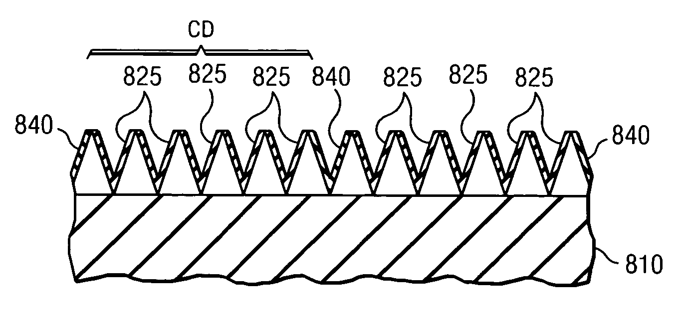
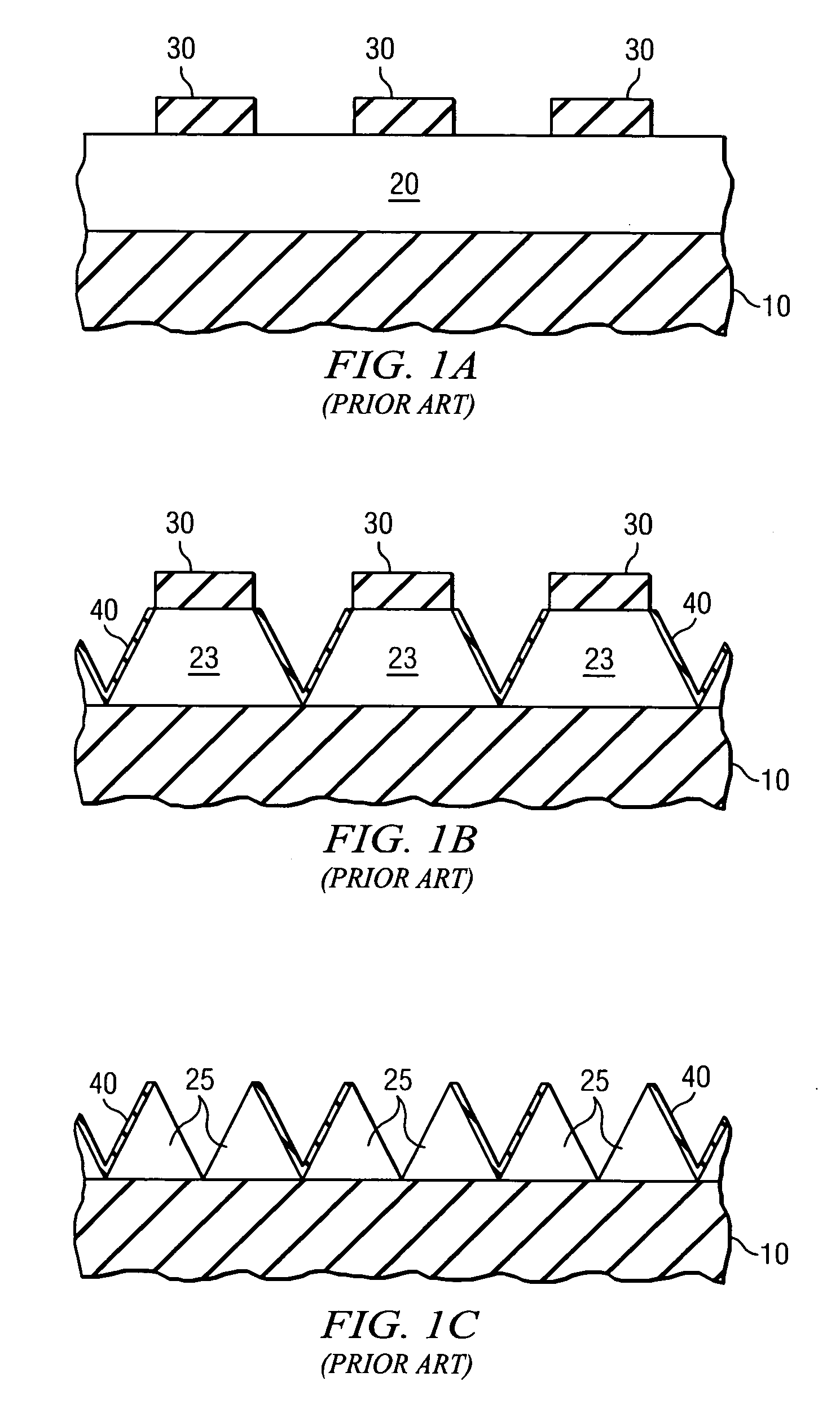
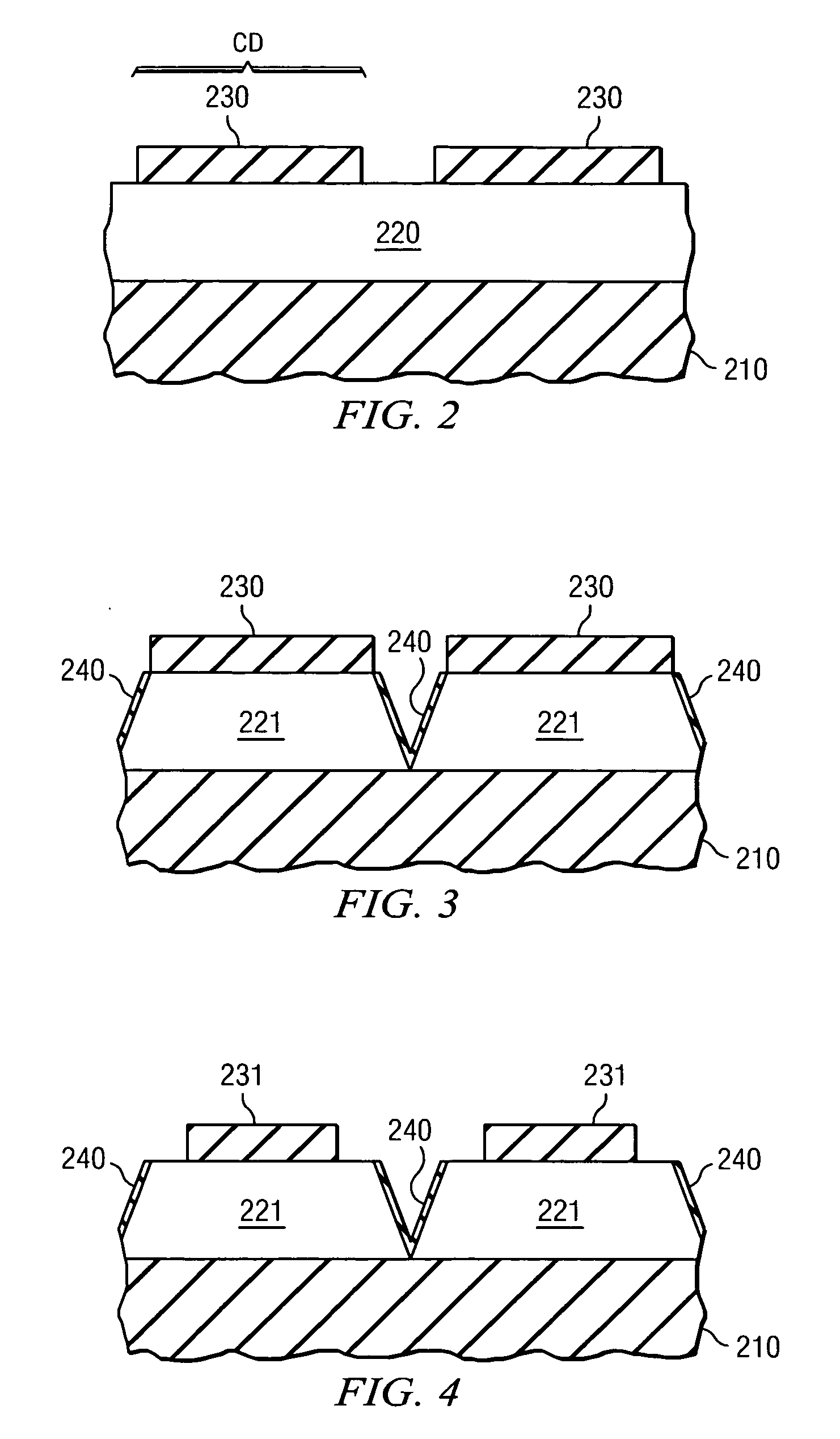
[0021]In the following description, reference is made to the accompanying drawings that form a part thereof, and in which is shown by way of illustration specific exemplary embodiments in which the invention may be practiced. These embodiments are described in sufficient detail to enable those skilled in the art to practice the invention and it is to be understood that other embodiments may be utilized and that changes may be made without departing from the scope of the invention. The following description is, therefore, not to be taken in a limited sense.

[0022]Notwithstanding that the numerical ranges and parameters setting forth the broad scope of the invention are approximations, the numerical values set forth in the specific examples are reported as precisely as possible. Any numerical value, however, inherently contains certain errors necessarily resulting from the standard deviation found in their respective testing measurements. Moreover, all ranges disclosed herein are to be...


PUM


Abstract

A method for multiplying the pitch of a semiconductor device is disclosed. The method includes forming a patterned mask layer on a first layer, where the patterned mask layer has a first line width. The first layer can then be etched to form a first plurality of sloped sidewalls. After removing a portion of the patterned mask so that the patterned mask layer has a second line width less than the first line width, the first layer can be etched again to form a second plurality of sloped sidewalls. The patterned mask layer can then be removed. The first layer can be etched again to form a third plurality of sloped sidewalls. The first plurality of sloped sidewalls, the second plurality of sloped sidewalls, and the third plurality of sloped sidewalls can form an array of parallel triangular channels.

Description

FIELD OF THE INVENTION[0001]The present invention relates to semiconductor devices and methods for decreasing a feature size of semiconductor devices. More particularly, the present invention relates to semiconductor devices and method for forming semiconductor devices with channel arrays having decreased line / space feature size and increased area for current flow.BACKGROUND OF THE INVENTION[0002]The desire for higher packing densities, faster circuit speed, and lower power dissipation has driven the scaling of semiconductor devices to smaller dimensions. Feature sizes for channel length, for example, have approached 0.1 μm (100 nm) for devices such as metal-oxide-semiconductor field effect transistors (MOSFETs). As the channel length of these devices decrease below 100 nm, however, problems arise.[0003]One problem is that the gate oxide thickness must be reduced in proportion to the channel length to control short-channel effects and maintain a good subthreshold turn-off slope. As ...

Claims


Application Information

Patent Timeline
Patent Type & Authority Patents(United States)
IPC IPC(8): H01L21/336
CPCH01L21/28123H01L29/1037H01L29/4236H01L29/78H01L29/78696H01L29/808H01L29/8086H01L29/045H01L29/0657H01L21/0274H01L21/31105H01L29/06H01L29/7869
Inventor VENUGOPAL, RAMESHWASSHUBER, CHRISTOPH
Owner TEXAS INSTR INC
Why Eureka
Try Eureka