
Silicon wafers and method of fabricating the same
a technology of silicon wafers and crystalline materials, applied in the direction of crystal growth process, polycrystalline material growth, chemistry apparatus and processes, etc., can solve the problem of bulk micro-defects (bmd) and other problems
- Summary
- Abstract
- Description
- Claims
- Application Information
AI Technical Summary
Benefits of technology
Problems solved by technology
Method used
Image

Examples
Embodiment Construction
[0057]Certain preferred embodiments will be described with reference to the accompanying drawings. Since these embodiments are provided only for the purpose of providing those of ordinary skilled in the art with an understanding of this disclosure, it will be noted that they may be modified in various manners and that the scope of this disclosure is not limited by the embodiment described herein.
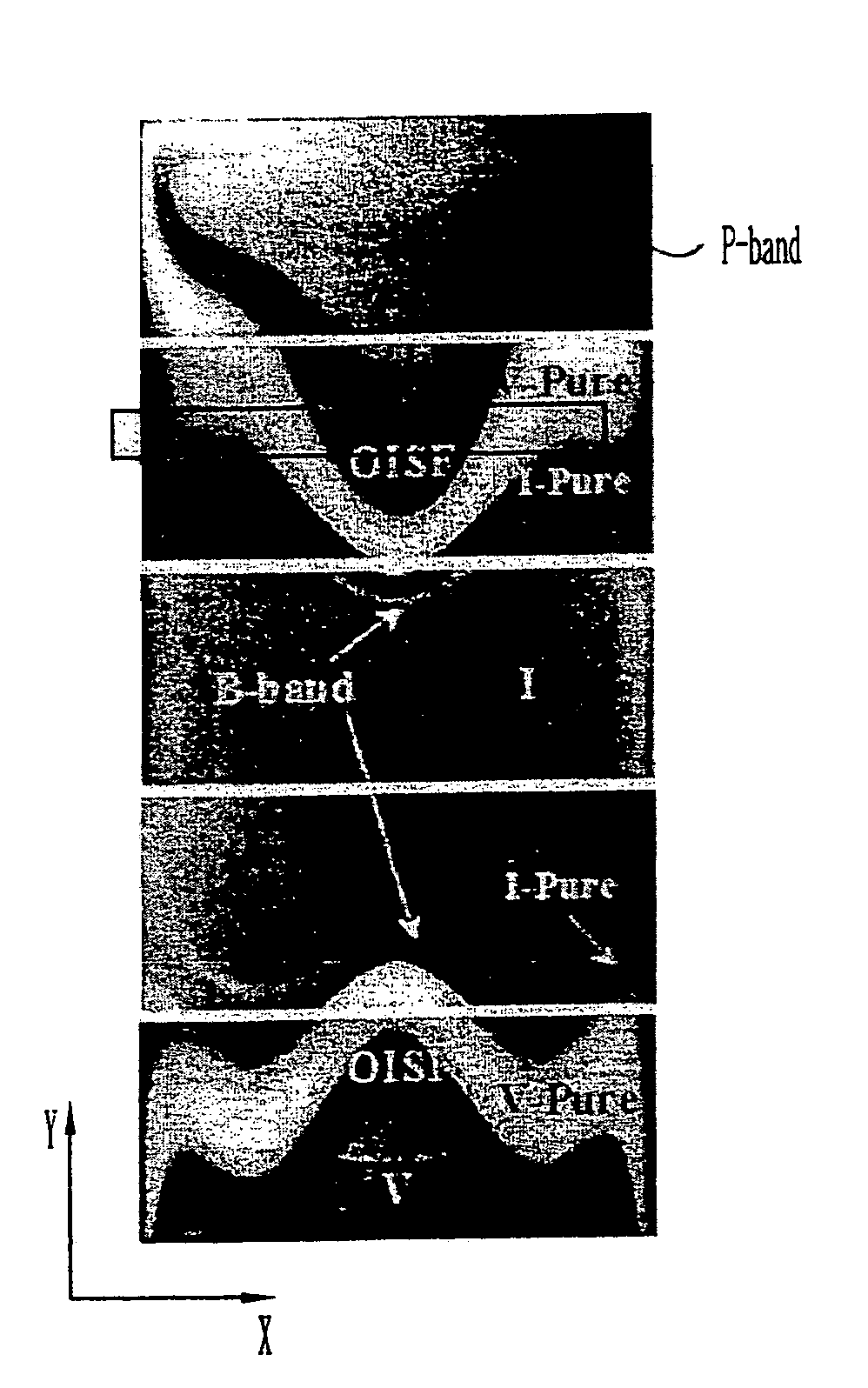
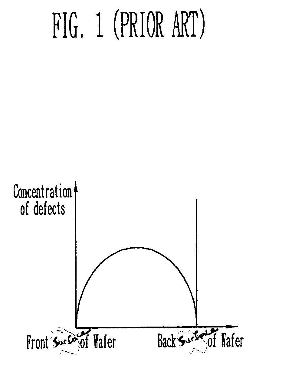
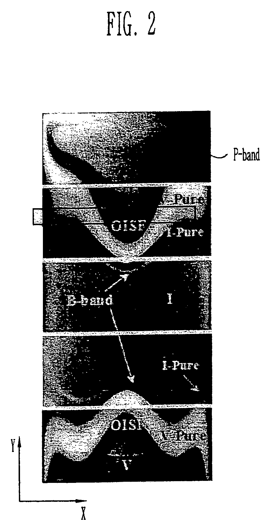
[0058]By using a two-step RTP (rapid thermal processing) process, a wafer with an ideal semiconductor device region is provided by controlling fine oxygen precipitates and OiSFs (Oxidation Induced Stacking Fault) located on the surface region of the wafer. By performing the two-step rapid thermal process, the distribution of defects can be accurately controlled and an ideal device active zone can be formed up to a certain depth from the surface of the wafer. In addition, it is possible to maximize the internal gettering (IG) efficiency by enabling the oxygen precipitates and the bulk stackin...
PUM
| Property | Measurement | Unit |
|---|---|---|
| distances | aaaaa | aaaaa |
| sizes | aaaaa | aaaaa |
| temperature | aaaaa | aaaaa |
Abstract
Description
Claims
Application Information