Circuit board inspection device

a technology of circuit board and inspection device, which is applied in the direction of measurement device, printed circuit testing, instruments, etc., can solve the problems of large labor cost, difficulty in restoring equipment, and difficulty in detecting various abnormalities or failures, etc., and achieve the effect of easy and accurate inspection

Inactive Publication Date: 2007-07-31
FUJIFILM BUSINESS INNOVATION CORP
View PDF20 Cites 26 Cited by
  • Summary
  • Abstract
  • Description
  • Claims
  • Application Information

AI Technical Summary

Benefits of technology

[0029]According to the invention, the signal change detection unit is disposed in a position of the supporting substrate corresponding to a part or a wire of the circuit board. Thus, when the supporting substrate on which the signal change detection unit is disposed is disposed substantially in parallel with the circuit board, the signal change detection unit is aligned with the part or the wire so that the part or the wire mounted on the circuit board can be inspected easily and accurately. In addition, the signal change detection unit is disposed on the supporting substrate without necessity of incorporating the signal change detection unit in the circuit board. Thus, the signal change detection unit can be disposed in accordance with the parts layout of the circuit board to be inspected, so that the signal change detection unit can be applied to an existing circuit board.

Problems solved by technology

Particularly in a bad environment where the equipment is used, various abnormalities or failures difficult to be detected may occur in spite of normal use.
Thus, a great deal of labor is required for restoring the equipment.
Even when the equipment is used in a normal environment, there may occur an abnormality or a failure in the electronic circuits.
Further, once there occurs an abnormality in the electronic circuit boards, a prompt countermeasure must be taken in view of safety, cost and so on.
However, when there occurs abnormality or failure as described previously, the equipment is usually out of commission, causing a downtime disadvantageously to the user side.
That is, it may take much labor to specify the failure location, or it is not always possible to specify the failure location correctly.
Thus, it may cost a great deal to exchange all the possible parts for the failure.
Alternatively, it may take much time for repair per se, or action to be taken may be delayed due to limited manpower.
Thus, in fact, both the user side and the maker side are often in a situation leading to a great loss.
When the magnetic field detection probe scans wiring of a board in a non-contact manner, abnormalities occurring in an existing high-density wiring printed board, including failures of ICs as well as disconnection / line-width abnormalities of the wiring in the board are detected in a high-speed and mechanical-stress-free state.
However, such a circuit board inspection device has the following problems.
That is, according to the technique disclosed in “Detection of Flaws in a Printed Circuit Board by Using an Eddy-Current Testing Approach”, the conditions of a signal line on the circuit board or the magnetic field generated from the current flowing through the signal line can be sensed in a non-contact manner and with high accuracy, but an exclusive probe used as means for sensing the magnetic field is so expensive that it costs much to detect a failure.
Thus, there occurs a problem that it takes much time or much labor to inspect a failure over the whole area of the circuit board.
Thus, there occurs a problem that the technique is poor in flexibility of arrangement.
Since various locations have to be measured in such a diagnosis method, there is however a problem that it takes much labor for failure diagnosis to thereby result in deterioration of working efficiency.
On the other hand, with the recent improvement of performance and function, the operation of electronic circuits becomes more and more complicated.
As a result, there is a problem that the number of man-hours for design increases so that the cost of the electronic circuits increases.
However, according to the method disclosed in Patent Document 1, the conditions of a signal line on the circuit board or the magnetic field generated from the current flowing through the signal line can be sensed in a non-contact manner and with high accuracy, but an expensive exclusive probe (sensing probe) has to be used as means for sensing the magnetic field.
Thus, it costs much to detect a failure.
It is therefore difficult to perform measurement in the state where the electronic circuit board is installed in a system such as electronic equipment, and it is necessary to perform failure diagnosis over the electronic circuit board off-line.
As a result, it has to take much time and much labor.
In addition, it is difficult to fix the position relation between the probe and the portion to be inspected.
Thus, it is difficult to perform accurate inspection.
However, it costs a great deal for such a case.
Thus, the related-art failure diagnosis method is not always user-friendly in view of the cost and the degree of freedom in setting a portion to be failure-diagnosed.

Method used


Image

  • Circuit board inspection device
  • Circuit board inspection device
  • Circuit board inspection device

Examples


first embodiment

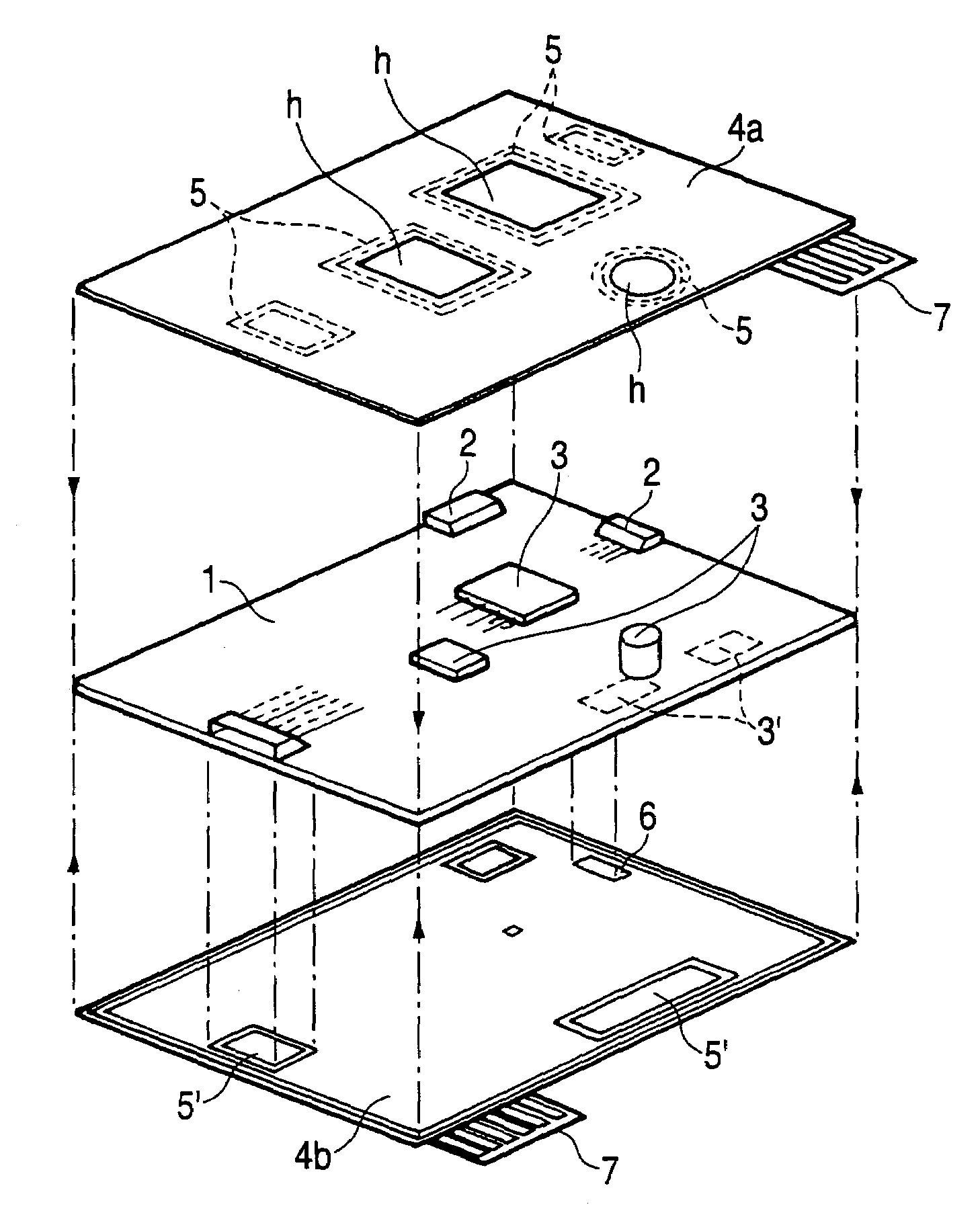
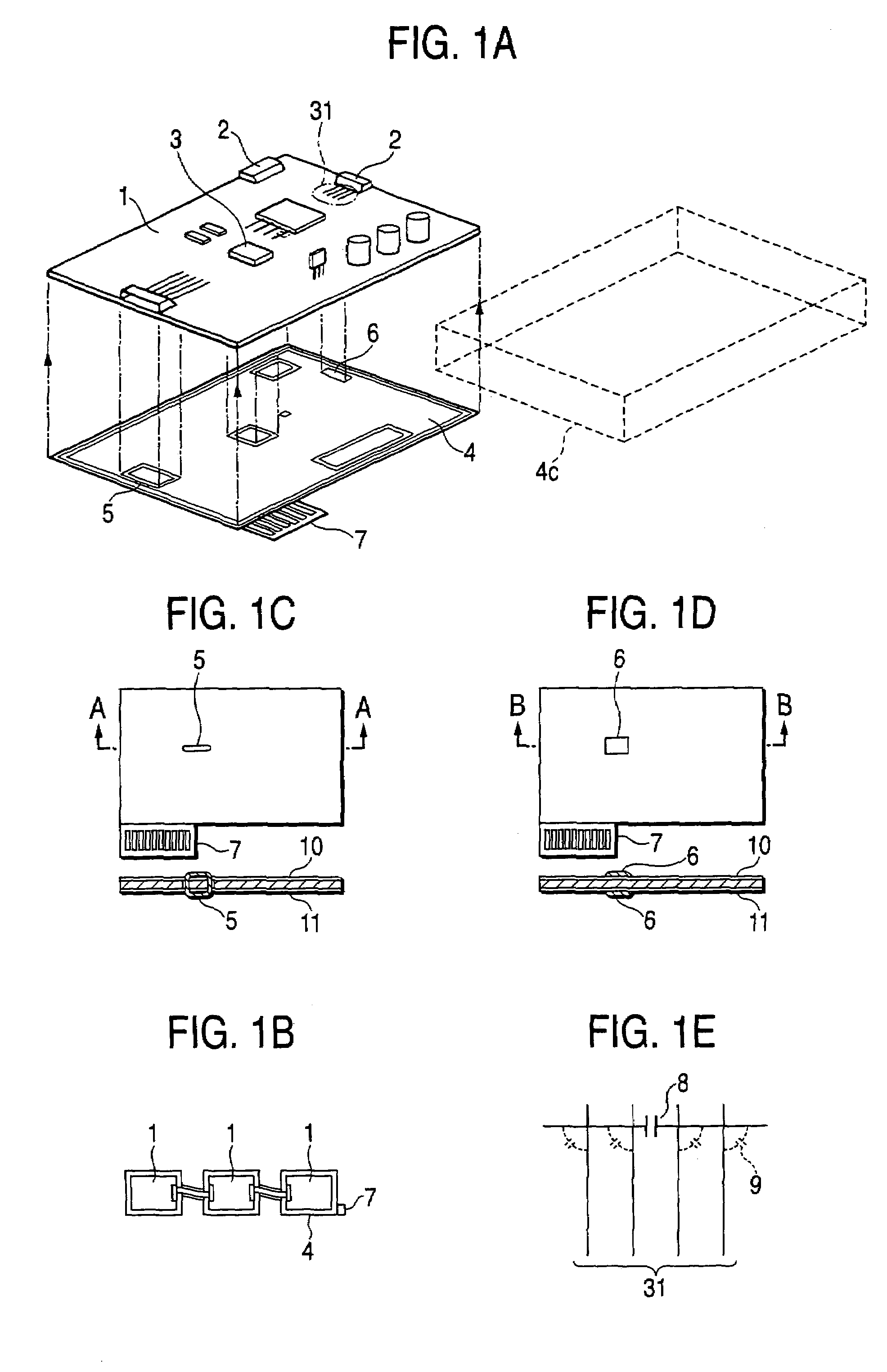
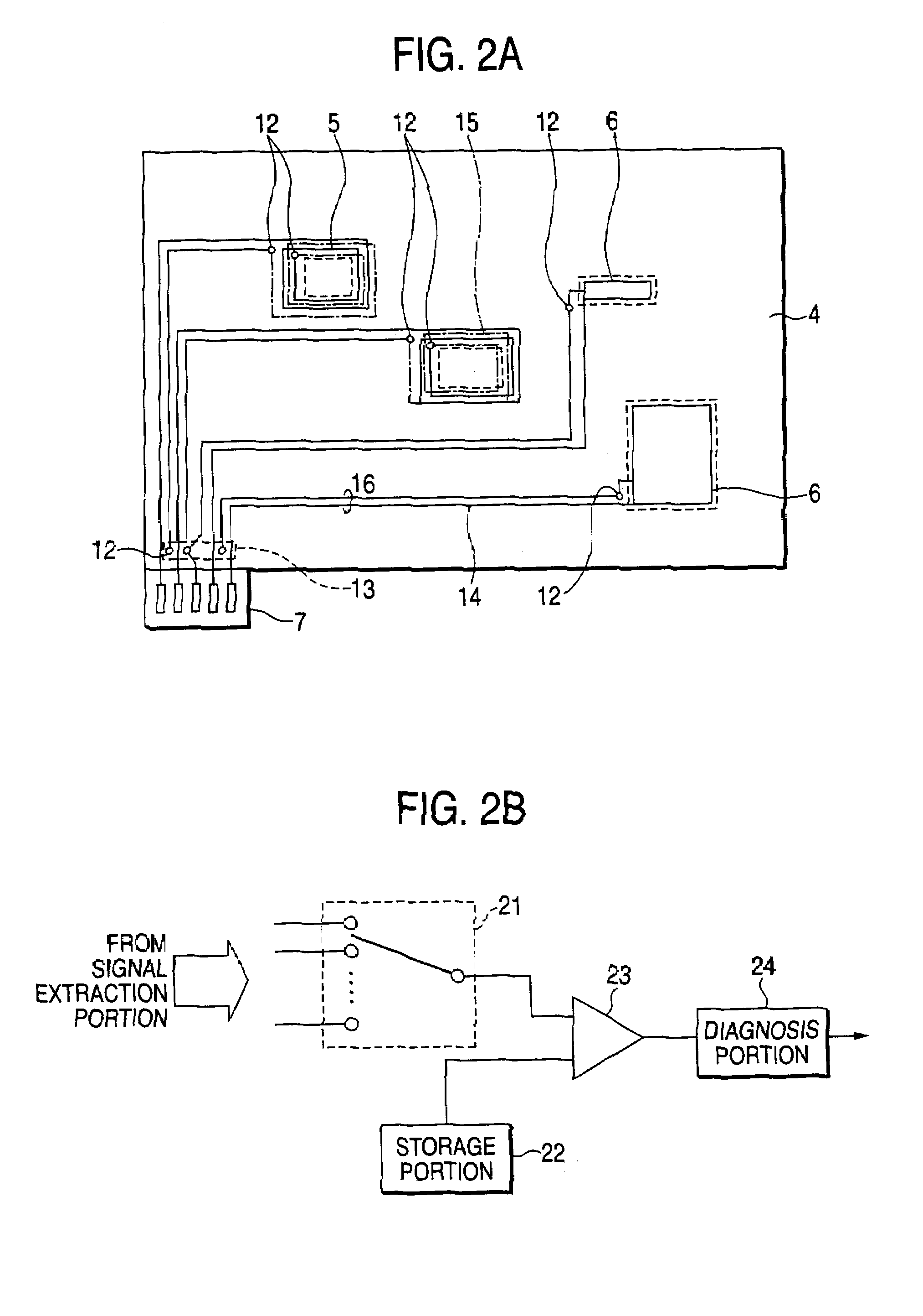
[0060]An embodiment of the invention will be described below with reference to the drawings. FIGS. 1A–1E and FIGS. 2A–2B are diagrams for explaining a circuit board inspection device according to this embodiment. FIGS. 3A–3B are diagrams for explaining inspection. The circuit board inspection device according to this embodiment is to inspect the operation of a circuit board 1 having a predetermined part 3 or wire formed thereon. The circuit board inspection device includes a supporting substrate 4 and a signal change detection unit (a coil 5 or a capacitor 6). The supporting substrate 4 is disposed substantially in parallel with the parts mounting surface of the circuit board 1. The signal change detection unit is disposed in a position of the supporting substrate 4 corresponding to the part 3 or wire of the circuit board 1, with the supporting substrate 4 being disposed substantially in parallel with the circuit board 1.

[0061]The signal change detection unit has a coil for generati...

second embodiment

[0097]FIG. 10 is a schematic perspective view for explaining another embodiment of a circuit substrate inspection device. The circuit substrate inspection device has a front-side supporting substrate 4a and a back-side supporting substrate 4b as supporting substrates disposed substantially in parallel with the parts mounting surface of the circuit board 1. The front-side supporting substrate 4a is disposed on the front side of the circuit board 1, and the back-side supporting substrate 4b is disposed on the back side of the circuit board 1.

[0098]This circuit board inspection device deals with a circuit board 1 to be inspected, in which parts 3 and wires connected to connectors 2 are provided on the opposite, front and back sides of the circuit board 1. In the circuit board inspection device, signal change detection units are disposed on the front-side supporting substrate 4a correspondingly to the positions of parts and the like disposed on the front side of the circuit board 1. On ...

third embodiment

[0118]FIG. 14 is a diagram for explaining the fundamental configuration and operation for implementing the invention. Wiring patterns 126 are formed on the surface of a circuit board (printed board) 110 mounted with not-shown circuit members including passive parts such as resistive elements, inductive elements and capacitive elements, or active parts such as transistors and ICs (Integrated Circuits). In the example shown in FIG. 1, two wiring patterns 126a and 126b are disposed adjacently at a predetermined distance.

[0119]The wiring patterns 126a and 126b are chiefly microstrip lines, generating magnetic fields from currents flowing through their wires as shown in FIG. 14. A spiral coil (inductor shaped like a spiral coil) 130 whose magnetic path length LEN is substantially equal to the width PW of the wiring pattern is disposed above one wiring pattern 126a so as to be close to the wiring pattern 126a in a non-contact manner and so as to be perpendicular to the direction of a curr...


PUM


Abstract

A circuit board inspection device for inspecting the operation of a circuit board having a predetermined part or wire formed therein includes a supporting substrate disposed substantially in parallel with the parts mounting surface of the circuit board, and a signal change detection unit made of a coil or a capacitor disposed in a position of the supporting substrate corresponding to the part or wire of the circuit board, with the supporting substrate being disposed substantially in parallel with the circuit board.

Description

[0001]The present disclosure relates to the subject matter contained in Japanese Patent Application No. 2002-367791 filed Dec. 19, 2002, Japanese Patent Application No. 2002-369283 filed Dec. 20, 2002, and Japanese Patent Application No. 2003-177697 filed Jun. 23, 2003, which are incorporated herein by reference in their entirety.BACKGROUND OF THE INVENTION[0002]1. Field of the Invention[0003]The present invention relates to a device for detecting or diagnosing an abnormal / failure state of an electronic circuit, and particularly relates to a circuit board inspection device for predicting, detecting or preventing abnormality / failure in operation or performance of an electronic circuit, for example, in equipment having the electronic circuit which is called PWBA formed out of a plurality of circuit boards connected with one another.[0004]Also, the present invention relates to a method for performing prediction or detection of abnormality or failure in operation or performance (hereina...

Claims


Application Information

Patent Timeline
Patent Type & Authority Patents(United States)
IPC IPC(8): G01R31/02G01R31/28G01R31/315
CPCG01R31/281G01R31/2818G01R31/315
Inventor NAKAGAWA, EIGOADACHI, KOJIYASUKAWA, KAORUYAMADA, NORIKAZUUWATOKO, KOKISATONAGA, TETSUICHI
Owner FUJIFILM BUSINESS INNOVATION CORP
Why Eureka
Try Eureka