Image forming apparatus featuring a variable oscillating electric field formed between a developer carrying member and an image bearing member during a developer operation in accordance with a peripheral speed of the image bearing member
a technology of image bearing and developer, which is applied in the direction of electrographic process apparatus, instruments, optics, etc., can solve the problems of prior art such as the above described, and achieve the effect of high quality
- Summary
- Abstract
- Description
- Claims
- Application Information
AI Technical Summary
Benefits of technology
Problems solved by technology
Method used
Image
Examples
embodiment 1
[General Structure and Operation of Image Forming Apparatus]
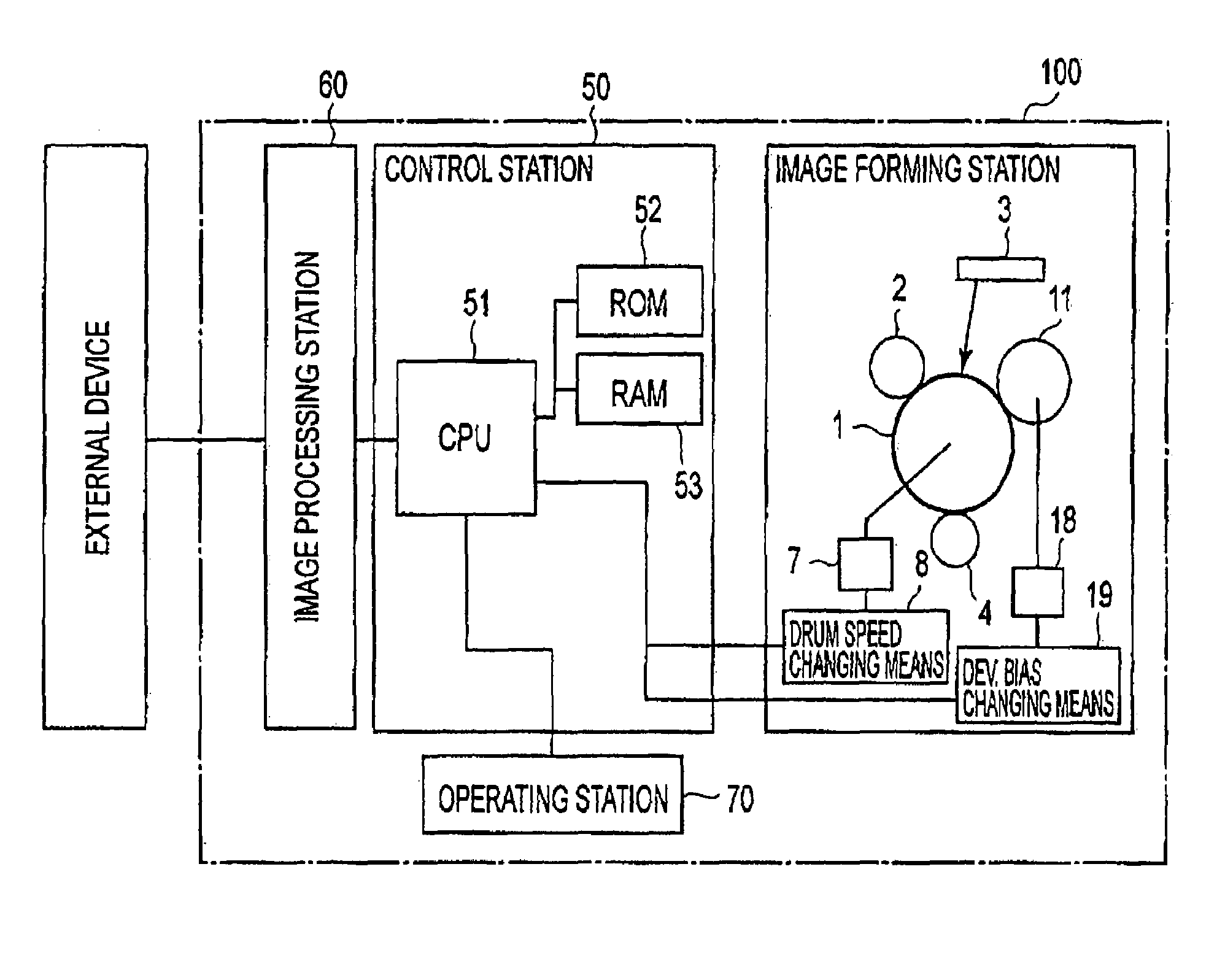
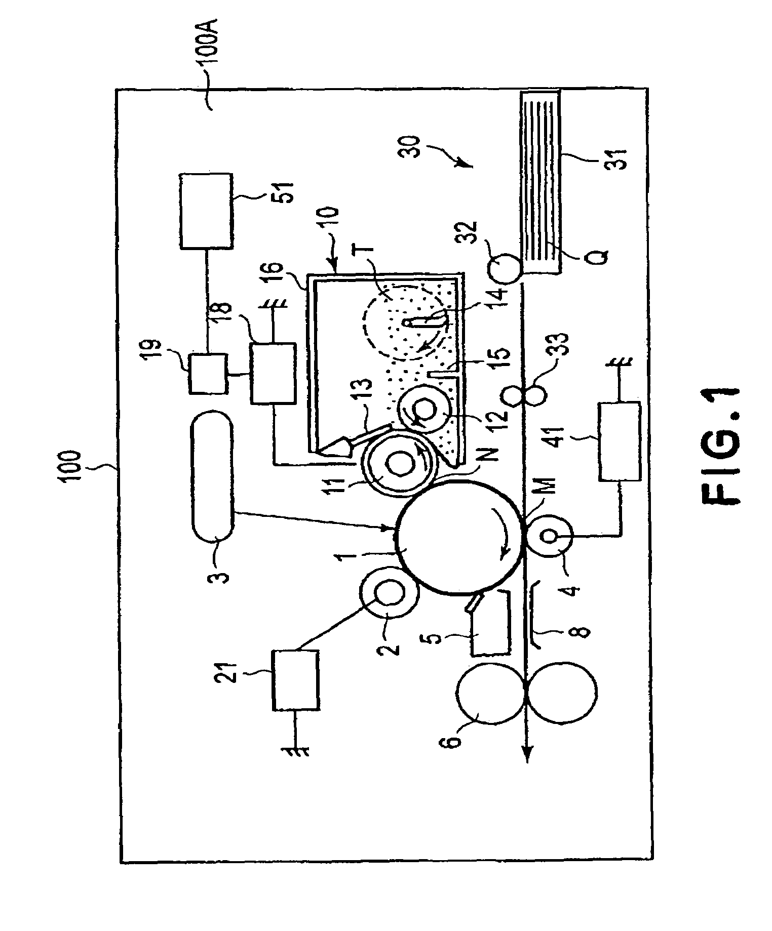
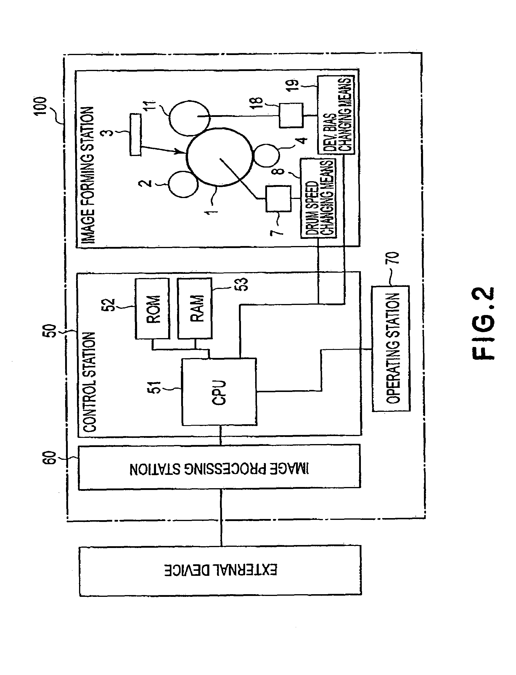
[0051]First, referring to FIG. 1, the general structure and operation of the image forming apparatus in the first embodiment of the present invention will be described. The image forming apparatus 100 in this embodiment is a laser beam printer capable of forming a full-color image, based on four color components, on recording medium such as recording paper, OHP sheet, fabric, etc., with the use of one of the electrophotographic image formation methods, in response to the image formation signals from a host such as a personal computer connected to the main assembly 100A of the image forming apparatus 100, or an external apparatus such as an original reading apparatus connected to the main assembly 100A and capable of optically reading an original and converting the obtained information about the original into electrical signals.
[0052]The image forming apparatus 100 has the rotatable photosensitive drum 1 as an image bearing ...
embodiment 2
[0094]Next, another embodiment, or the second embodiment, of the present invention will be described. The basic structure and operation of the image forming apparatus in this embodiment are virtually the same as those in the first embodiment. Thus, the components of the image forming apparatus in this embodiment, which are virtually identical or equivalent in structure and function to those in the first embodiment, are given the same referential symbols as those given for the description of the first embodiment, and will not be described in detail.
[0095]Referring to FIG. 6, also in this embodiment, a combination of AC and DC voltages is used as development bias. In this embodiment, however, AC and DC voltages are combined in such a manner that the development bias is provided with portions in which voltage oscillates and forms an oscillatory electric field, that is, an electrical field in which potential level alternates, and portions in which voltage does not oscillate, and therefo...
embodiment 3
[0126]Next, another embodiment, or the third embodiment, of the present invention will be described. The basic structure and operation of the image forming apparatus in this embodiment are virtually the same as those in the first embodiment. Thus, the components of the image forming apparatus in this embodiment, which are virtually identical or equivalent in structure and function to those in the first embodiment, are given the same referential symbols as those given for the description of the first embodiment, and will not be described in detail.
[0127]In this embodiment, the image forming apparatus is controlled in density by controlling the speed of the development roller 11. More specifically, the image forming apparatus 100 in this embodiment is enabled to operate in the low speed printing mode, standard mode, and high speed printing mode. In the low speed printing mode, the ratio of the peripheral velocity of the development roller 11 relative to that of the photosensitive drum...
PUM
 Abstract
Description
Claims
Application Information


