
Technology migration for integrated circuits with radical design restrictions

Inactive Publication Date: 2007-08-14
GLOBALFOUNDRIES INC
View PDF8 Cites 12 Cited by
  • Summary
  • Abstract
  • Description
  • Claims
  • Application Information

AI Technical Summary

Benefits of technology

[0007]The invention includes a method, system and program product for migrating an integrated circuit design from a source technology without RDR to a target technology with RDR. The invention implements a minimum layout perturbation approach that addresses RDR. The invention also solves the problem of inserting one or more dummy shapes where required, and extending the lengths of the critical shapes and / or the dummy shapes to meet “edge coverage” requirements.

Problems solved by technology

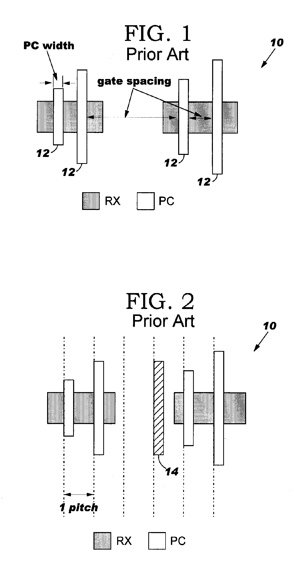
However, as technology is progressing into the sub-wavelength regime, new layout challenges have emerged in the form of groupings of fundamental design restrictions, which is sometimes referred to in the art as “radical design restrictions” (hereinafter “RDR”).
This regular design style presents a new challenge to the design migration solution, and demands new functionalities in the existing design migration software.

Method used


Image

  • Technology migration for integrated circuits with radical design restrictions
  • Technology migration for integrated circuits with radical design restrictions
  • Technology migration for integrated circuits with radical design restrictions

Examples


Embodiment Construction

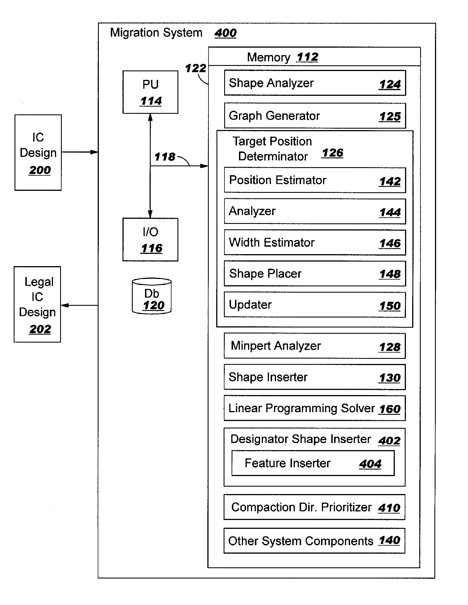
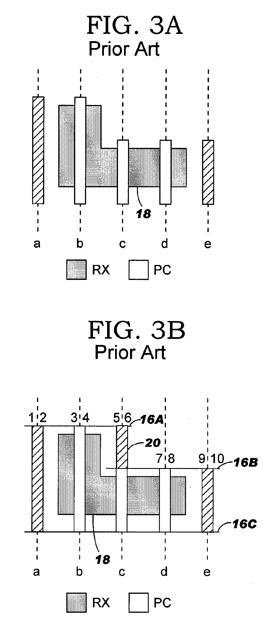
[0041]The invention includes a system, method and program product for migrating an integrated circuit (IC) design from a source technology without RDR to a target technology with RDR. Although RDRs are currently only required for critical gates, the invention is applicable to legalize shapes with similar constraints, such as metal wiring shapes. Therefore, the term “critical shapes” will be used herein to refer to gates, PC shapes or metal wiring shapes, which are required to meet the grid constraints. Critical shapes are to be differentiated from “dummy shapes,” which the invention may insert to make an IC design legal, and meet a design rule requirement.

[0042]In evaluating RDR, a gate is formed by the intersection between a polysilicon-conductor (PC) shape and a diffusion region (RX). “Pitch” is defined as the spacing between the centerlines of two adjacent gates. “Critical gates” are those that must comply with RDR in order to be properly printed in the manufacturing process. Usu...


PUM


Abstract

A method, system and program product for migrating an integrated circuit (IC) design from a source technology without radical design restrictions (RDR) to a target technology with RDR, are disclosed. Also, a method, system and program product for migrating an integrated circuit design from a source technology without RDR to a target technology with RDR in which space may be reserved for late insertion of a feature and in which migration first occurs in a primary compaction direction having less tolerant ground rules.

Description

[0001]This application is a continuation-in-part of U.S. Ser. No. 10 / 904,225, filed Oct. 29, 2004, currently pending.BACKGROUND OF THE INVENTION[0002]1. Technical Field[0003]The present invention relates generally to technology migration for integrated circuits (ICs), and more particularly, to a method, system and program product for technology migration for an IC with radical design restrictions.[0004]2. Related Art[0005]Design migration is an essential process to achieve maximum layout productivity in very large-scale integrated (VLSI) circuit designs. Conventional graph-based compaction techniques were developed to translate a symbolic layout to a physical layout based on simplistic edge-based ground rules. These techniques have also been used to solve the design migration problem. More recently, a minimum layout perturbation formulation of the design migration problem results in a method that preserves the integrity of the source layout. While existing design migration software ...

Claims


Application Information

Patent Timeline
Patent Type & Authority Patents(United States)
IPC IPC(8): G06F17/50
CPCG06F17/5068G06F17/5077G06F30/39G06F30/394
Inventor ALLEN, ROBERT J.ENDICOTT, CAM V.HENG, FOOK-LUENHIBBELER, JASON D.MCCULLEN, KEVIN W.NARAYAN, RANIWALKER, ROBERT F.YUAN, XIN
Owner GLOBALFOUNDRIES INC
Learn More