Methods for forming interconnects in microelectronic workpieces and microelectronic workpieces formed using such methods

a microelectronic workpiece and microelectronic technology, applied in the direction of semiconductor devices, electrical apparatus, semiconductor/solid-state device details, etc., can solve the problems of reducing the size of high-performance devices, forming wire-bonds b>13/b> in stacked devices, and larger ball-grid arrays

Active Publication Date: 2007-09-18
MICRON TECH INC
View PDF101 Cites 95 Cited by
  • Summary
  • Abstract
  • Description
  • Claims
  • Application Information

AI Technical Summary

Problems solved by technology

Reducing the size of high-performance devices, however, is difficult because the sophisticated integrated circuitry of such devices requires more bond-pads, which results in larger ball-grid arrays and thus larger footprints.
Forming the wire-bonds 13 in the stacked device shown in FIG. 1 can be complex and/or expensive because it requires placi

Method used


Image

  • Methods for forming interconnects in microelectronic workpieces and microelectronic workpieces formed using such methods
  • Methods for forming interconnects in microelectronic workpieces and microelectronic workpieces formed using such methods
  • Methods for forming interconnects in microelectronic workpieces and microelectronic workpieces formed using such methods

Examples


Embodiment Construction

A. Overview

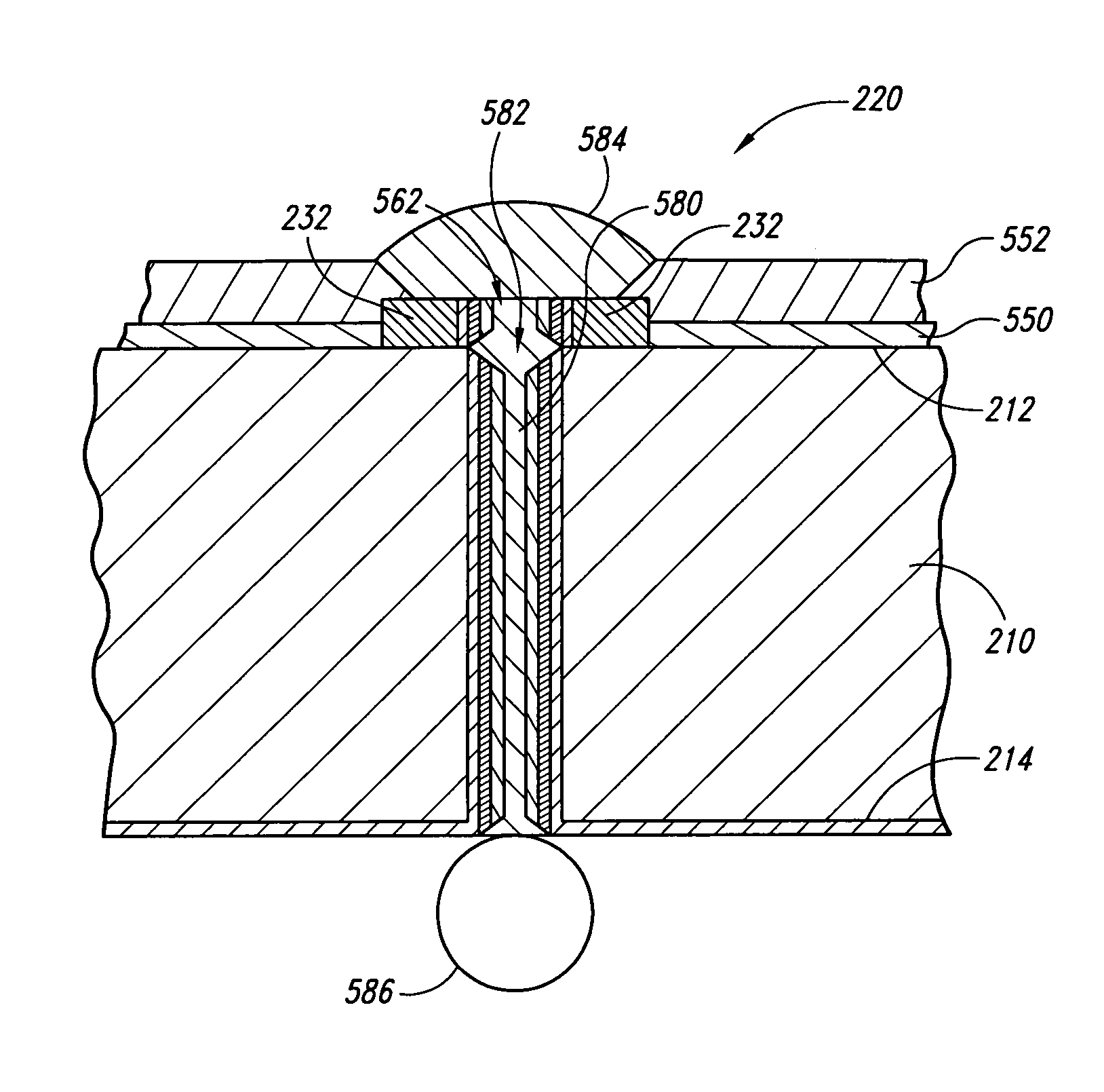
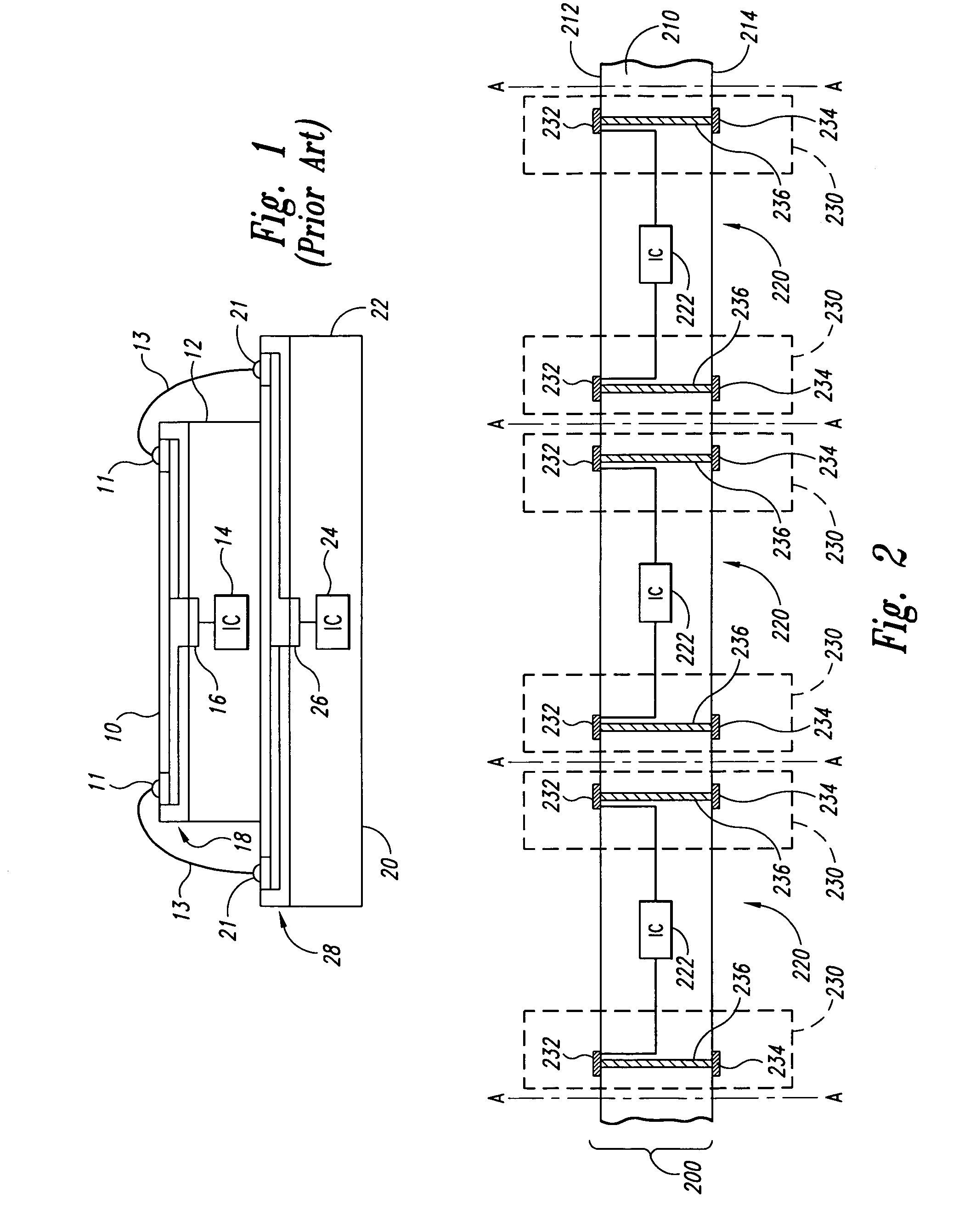
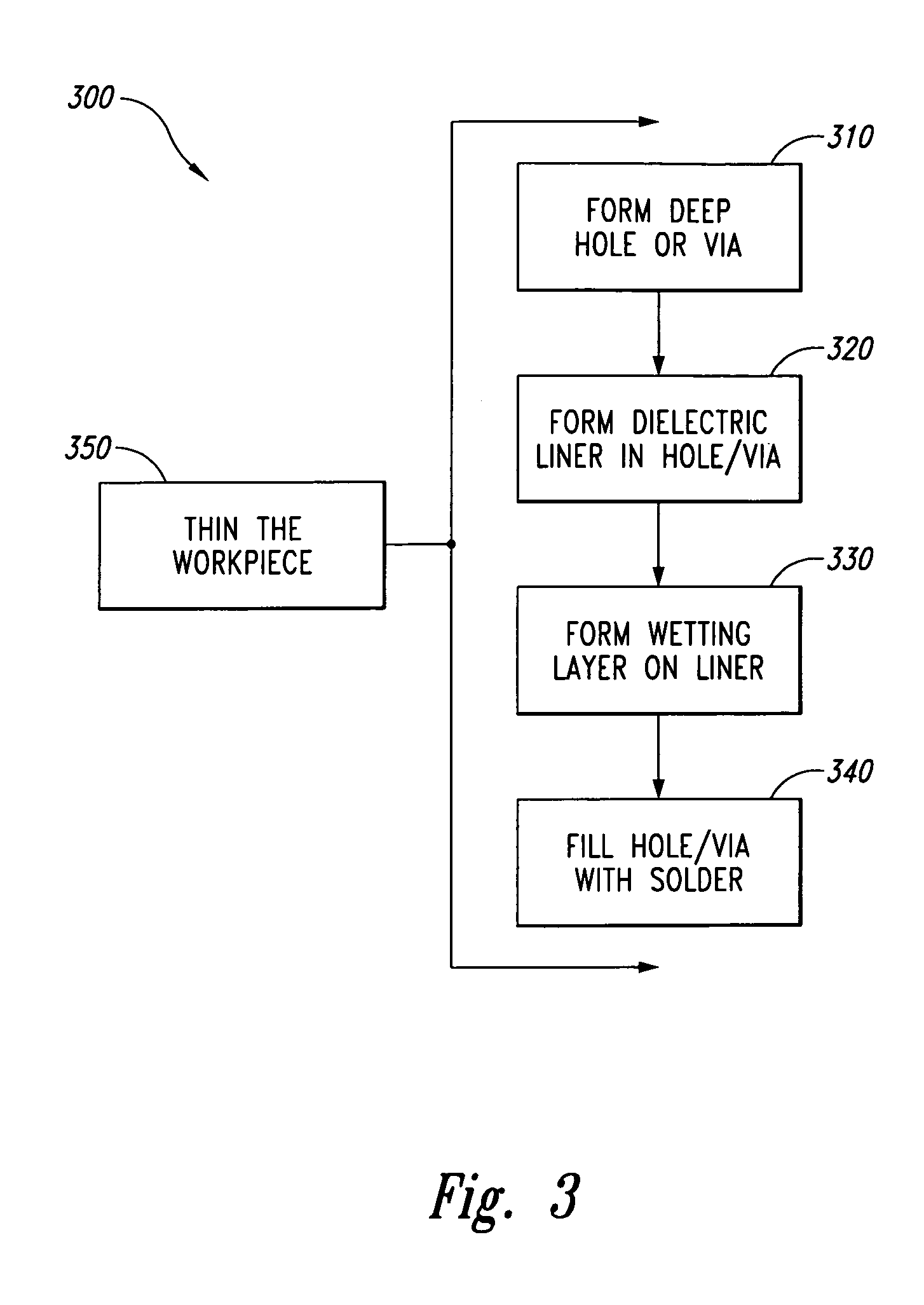
[0022]The following disclosure describes several embodiments of methods for forming electrically conductive through-wafer interconnects in microelectronic workpieces and microelectronic workpieces having such interconnects. Such interconnects electrically couple terminals or other conductive elements proximate to one side of the workpiece to conductive elements proximate to the other side of the workpiece. The following describes several embodiments of methods for forming interconnects in (1) through-holes extending through the workpiece, and (2) blind holes or vias extending to an intermediate depth in the workpiece.

[0023]One aspect of the invention is directed toward a method for manufacturing a microelectronic workpiece having a plurality of microelectronic dies. The individual dies include an integrated circuit and a terminal electrically coupled to the integrated circuit. In one embodiment, the method includes forming an opening in the workpiece in alignment with the...


PUM


Abstract

Methods for forming interconnects in microelectronic workpieces and microelectronic workpieces having such interconnects are disclosed herein. One aspect of the invention is directed toward a method for manufacturing a microelectronic workpiece having a plurality of microelectronic dies. The individual dies include an integrated circuit and a terminal electrically coupled to the integrated circuit. In one embodiment, the method includes forming an opening in the workpiece in alignment with the terminal. The opening can be a through-hole extending through the workpiece or a blind hole that extends only partially through the substrate. The method continues by constructing an electrically conductive interconnect in the workpiece by depositing a solder material into at least a portion of the opening and in electrical contact with the terminal. In embodiments that include forming a blind hole, the workpiece can be thinned either before or after forming the hole.

Description

APPLICATIONS INCORPORATED BY REFERENCE[0001]The present application is in a related area of subject matter as the following U.S. applications, which are incorporated herein by reference: U.S. application Ser. No. 10 / 879,398 entitled “Packaged Microelectronic Imagers and Methods of Packaging Microelectronic Imagers” filed Jun. 29, 2004; and U.S. application Ser. No. 10 / 864,974 entitled “Packaged Microelectronic Imagers and Methods of Packaging Microelectronic Imagers” filed Jun. 10, 2004.TECHNICAL FIELD[0002]The present invention relates to forming interconnects in microelectronic workpieces and microelectronic workpieces formed using such methods.BACKGROUND[0003]Conventional packaged microelectronic devices can include a singulated microelectronic die, an interposer substrate or lead frame attached to the die, and a molded casing around the die. The die generally includes an integrated circuit and a plurality of bond-pads coupled to the integrated circuit. The bond-pads are typicall...

Claims


Application Information

Patent Timeline
IPC IPC(8): H01L23/48H01L21/44
CPCH01L21/76898H01L23/481H01L25/0657H01L25/50H01L2224/32145H01L2225/06513H01L2924/0002H01L2225/06541H01L2224/0557H01L2224/05552
Inventor KIRBY, KYLE K.
Owner MICRON TECH INC
Why Eureka
Try Eureka