Examining a structure formed on a semiconductor wafer using machine learning systems

Inactive Publication Date: 2007-10-09
TOKYO ELECTRON LTD
View PDF10 Cites 52 Cited by
  • Summary
  • Abstract
  • Description
  • Claims
  • Application Information

AI Technical Summary

Problems solved by technology

However, these machine learning systems, which generate profiles as outputs based on diffraction signals received as inputs, can produce erroneous results when noise is present in the diffraction signals obtained from the optical metrology device, and when the machine learning system have been trained using a model that is not accurate enough to describe the actual profile of the structure.

Method used


Image

  • Examining a structure formed on a semiconductor wafer using machine learning systems
  • Examining a structure formed on a semiconductor wafer using machine learning systems
  • Examining a structure formed on a semiconductor wafer using machine learning systems

Examples


Embodiment Construction

[0014]The following description sets forth numerous specific configurations, parameters, and the like. It should be recognized, however, that such description is not intended as a limitation on the scope of the present invention or applications thereof, but instead provides examples and illustrations.

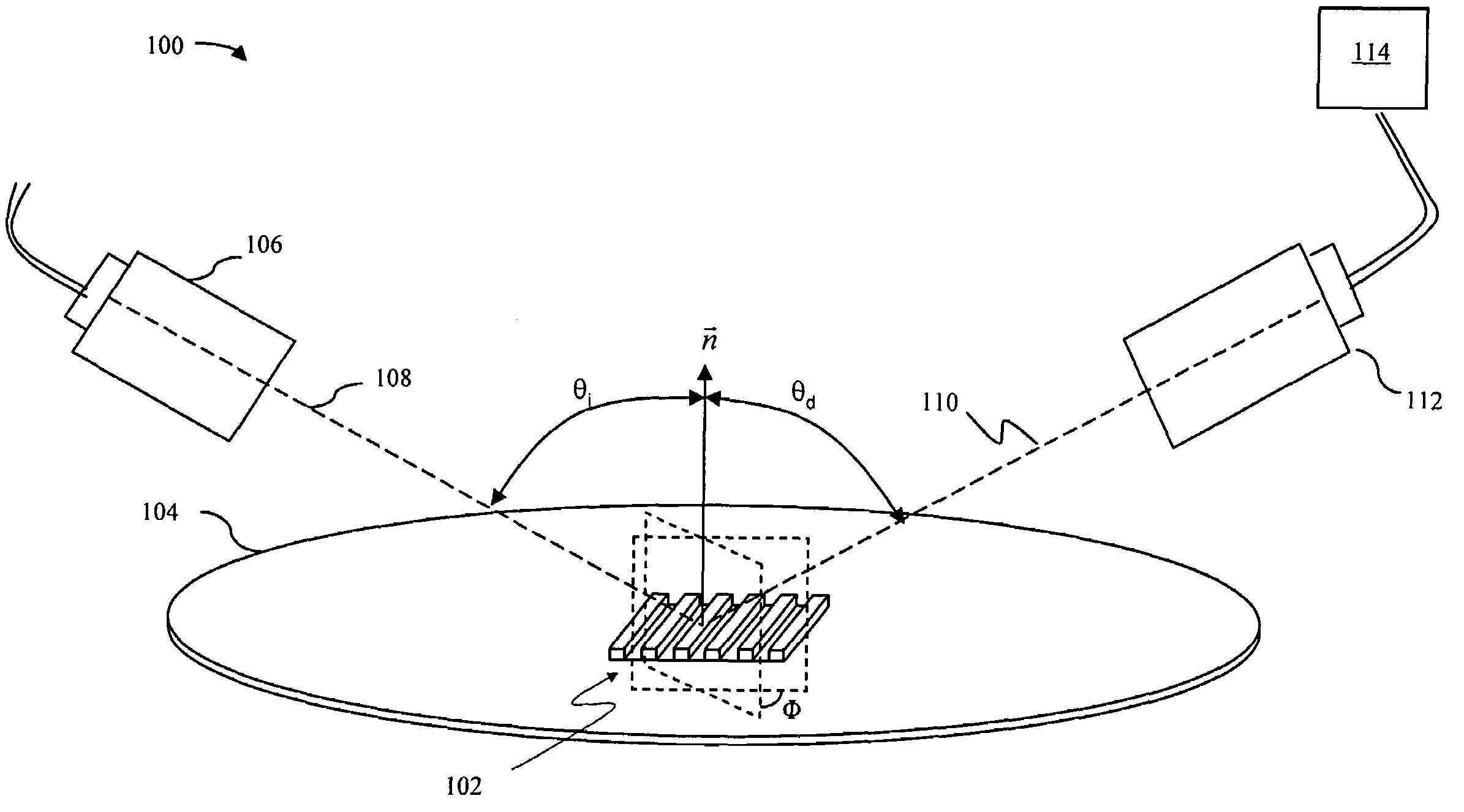
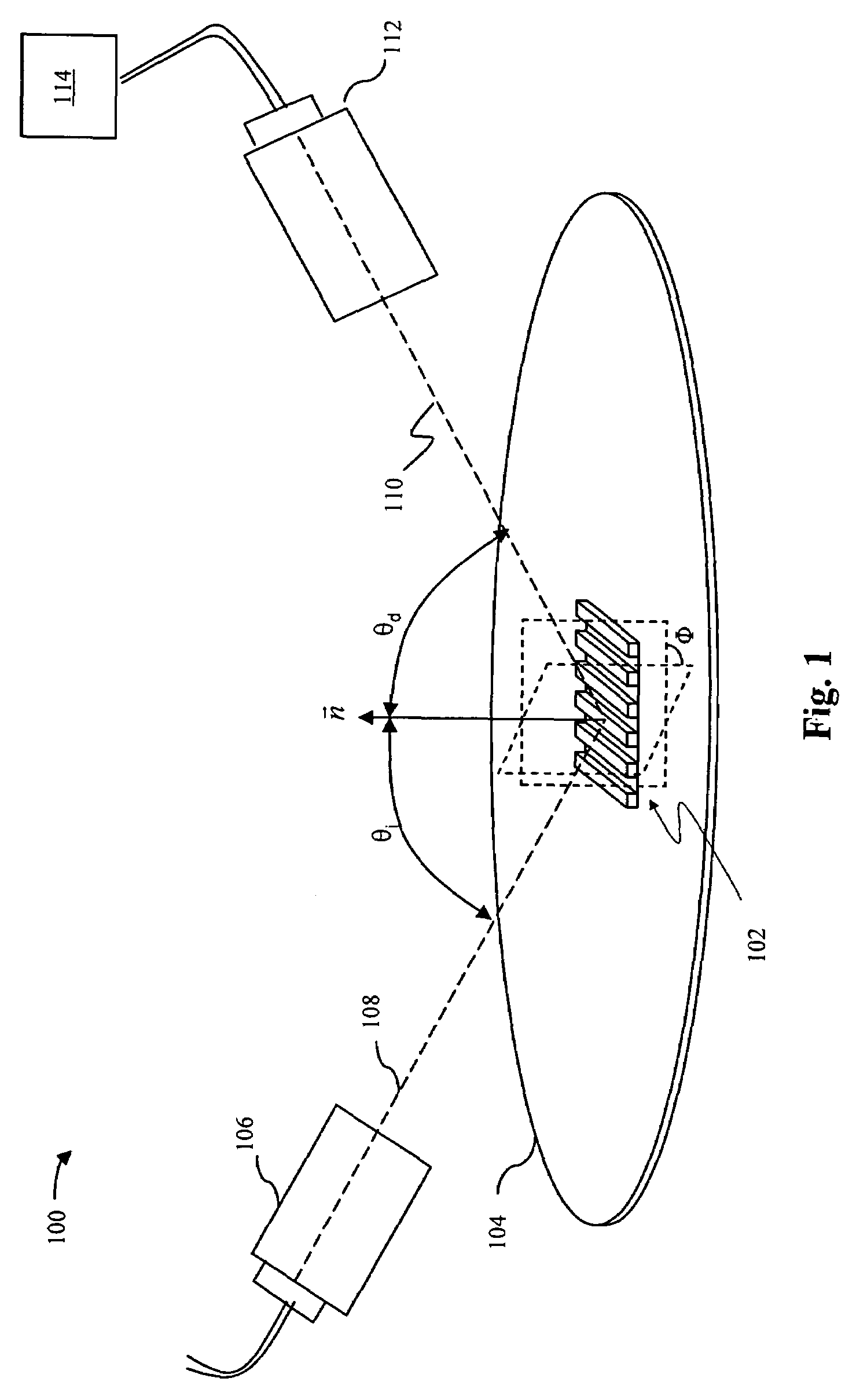
[0015]With reference to FIG. 1, a metrology system 100 can be used to examine a structure formed on a semiconductor wafer 104. For example, metrology system 100 can be used to determine a feature of a periodic grating 102 formed on wafer 104. Periodic grating 102 can be formed in test areas on wafer 104, such as adjacent to a device formed on wafer 104. In examples, periodic grating 102 can be formed in an area of the device that does not interfere with the operation of the device or along scribe lines on wafer 104. It should be recognized that the structure being examined can be any type of structure formed on wafer 104, including a feature of an integrated circuit device.
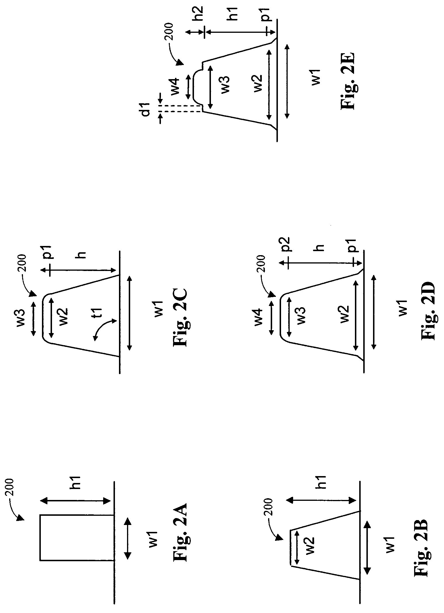
[0016]As depi...


PUM


Abstract

A structure formed on a semiconductor wafer is examined by obtaining a first diffraction signal measured from the structure using an optical metrology device. A first profile is obtained from a first machine learning system using the first diffraction signal obtained as an input to the first machine learning system. The first machine learning system is configured to generate a profile as an output for a diffraction signal received as an input. A second profile is obtained from a second machine learning system using the first profile obtained from the first machine learning system as an input to the second machine learning system. The second machine learning system is configured to generate a diffraction signal as an output for a profile received as an input. The first and second profiles include one or more parameters that characterize one or more features of the structure.

Description

BACKGROUND[0001]1. Field[0002]The present application relates to semiconductor wafer metrology, and, more particularly, to examining structures formed on semiconductor wafers using machine learning systems.[0003]2. Related Art[0004]In semiconductor manufacturing, metrology is typically used for quality assurance. For example, after fabricating a structure on a semiconductor wafer, a metrology system is used to examine the structure to evaluate the fabrication process utilized to form the structure. The structure can be a feature of an integrated circuit formed on the wafer, or a test structure, such as a periodic grating, formed adjacent to the integrated circuit.[0005]Optical metrology is a type of metrology that involves directing an incident optical signal at the structure, measuring the resulting diffraction signal, and analyzing the diffraction signal to determine a feature of the structure. Machine learning systems have been used to analyze diffraction signals obtained using a...

Claims


Application Information

Patent Timeline
Patent Type & Authority Patents(United States)
IPC IPC(8): G01B11/14G01B11/24G01B7/00
CPCG03F7/70625G03F1/84G03F1/0092
Inventor LI, SHIFANGBAO, JUNWEI
Owner TOKYO ELECTRON LTD
Why Eureka
Try Eureka