CCD device having a sequence of electrodes for charge multiplication

a ccd device and electrode technology, applied in the field of ccd imagers, can solve the problems of limited sensitivity of such a device, and the gain performance of such a ccd device can deteriorate with time of use, so as to prevent or reduce the buildup of trapped charge

Active Publication Date: 2007-11-06
E2V TECH (UK) LTD
View PDF1 Cites 32 Cited by
  • Summary
  • Abstract
  • Description
  • Claims
  • Application Information

AI Technical Summary

Benefits of technology

[0010]The additional charge density caused by doping choice alters the trajectory of electrons within the semiconductor due to the modified potential distribution within the silicon and prevents electrons encountering the surface of the semiconductor. This prevents or reduces build up of trapped charge which would otherwise degrade the gain performance of the device for a given voltage bias applied.

Problems solved by technology

The sensitivity of such a device is limited by the noise of the charge to voltage conversion process and that introduced by the subsequent video chain electronics.
In particular, we have appreciated that the gain performance of such a CCD device can deteriorate with time of use.

Method used


Image

  • CCD device having a sequence of electrodes for charge multiplication
  • CCD device having a sequence of electrodes for charge multiplication
  • CCD device having a sequence of electrodes for charge multiplication

Examples


Embodiment Construction

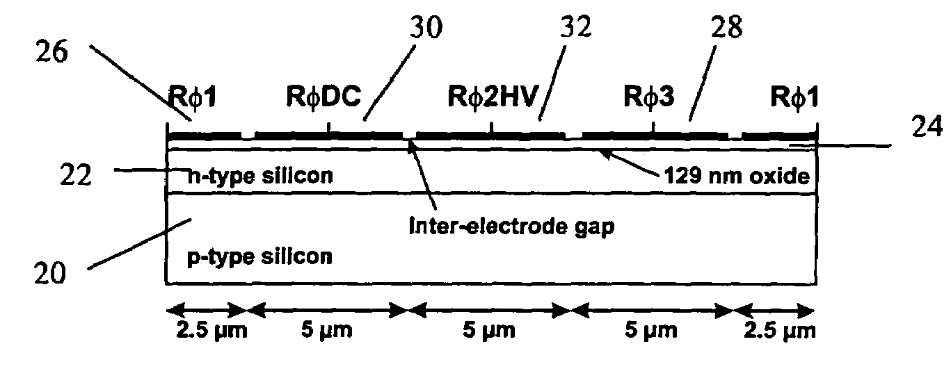
[0023]The present embodiment comprises a CCD device such as a CCD imager of known type but modified to change the doping arrangement of a multiplication element in a multiplication register. Such a known device is shown and has been described in relation to FIG. 1. The invention may be embodied in such a device, and in an imager or camera including such a device, and in an imager or camera including such a device.

[0024]As shown in FIG. 1, an image area 2 accumulates charge in CCD elements and transfers charge under control of clocked drive pulses on electrodes 7, 8 to a store area 3 and from the store area to an output register 4 and subsequently to a multiplication register 5. It is in the multiplication register that the invention is embodied, though it will be appreciated that other arrangements of multiplication elements could be used. Although shown as a straight line extension of the output register 4, in reality it will probably be bent around the imager for packaging reasons...


PUM


Abstract

A CCD device includes multiplication elements arranged so as to multiply charge by clocking with a high voltage. An additional region beneath the high voltage electrode is so doped in relation to at least the preceding electrode as to have a higher depleted charge density than under the preceding electrode. This assists in preventing high energy electrodes from encountering the silicon surface of the semiconductor.

Description

CROSS-REFERENCE TO RELATED APPLICATION[0001]This application claims the priority of British Patent Application No. 0506577.6 filed on Mar. 31, 2005, the subject matter of which is incorporated herein by reference.BACKGROUND OF THE INVENTION[0002]The present invention relates to a CCD device, and in particular to a CCD imager which provides gain in a CCD channel.[0003]In a typical CCD imager, signal charge representative of incident radiation is accumulated in an array of pixels in an image area. Following an integration period, signal charge is transferred to a store section and then to an output register by applying appropriate clocking or drive pulses to control electrodes. The signal charge is then read out from the output register and applied to a charge detection circuit to produce a voltage which is representative of the amount of signal charge. The sensitivity of such a device is limited by the noise of the charge to voltage conversion process and that introduced by the subse...

Claims


Application Information

Patent Timeline
Patent Type & Authority Patents(United States)
IPC IPC(8): H01L27/00H01L27/148H01L29/768
CPCH01L27/14806H01L29/76833H01L27/14831
Inventor ROBBINS, MARK STANFORD
Owner E2V TECH (UK) LTD
Why Eureka
Try Eureka