Apparatus and method for making circuitized substrates in a continuous manner

a technology of circuitized substrates and apparatuses, applied in the direction of printed circuit manufacturing, printed circuit aspects, conductive pattern formation, etc., can solve the problems of expensive transfer and time-consuming, and achieve the effect of enhancing the circuitized substrate ar

Inactive Publication Date: 2007-11-13
I3 ELECTRONICS
View PDF36 Cites 18 Cited by
  • Summary
  • Abstract
  • Description
  • Claims
  • Application Information

AI Technical Summary

Benefits of technology

[0037]It is, therefore, a primary object of the present invention to enhance the circuitized substrate art by providing a new and unique method of producing such substrates.
[0038]It is another object of the invention to provide such a process in which several conductive thru holes are formed to interconnect various conductive layers of the substrate.
[0039]It is still another object of the invention to provide such a process which can be implemented using conventional printed circuit board technologies.

Problems solved by technology

Such transfer is costly and time-consuming, especially when involving multi-layered products, the most common of boards sold today in view of increased operational demands for the products (e.g., computer servers, mainframes, etc.) in which such boards are implemented.

Method used


Image

  • Apparatus and method for making circuitized substrates in a continuous manner
  • Apparatus and method for making circuitized substrates in a continuous manner
  • Apparatus and method for making circuitized substrates in a continuous manner

Examples


Embodiment Construction

[0046]For a better understanding of the present invention, together with other and further objects, advantages and capabilities thereof, reference is made to the following disclosure and appended claims in connection with the above-described drawings. It is understood that like numerals will be used to indicate like elements from FIG. to FIG.

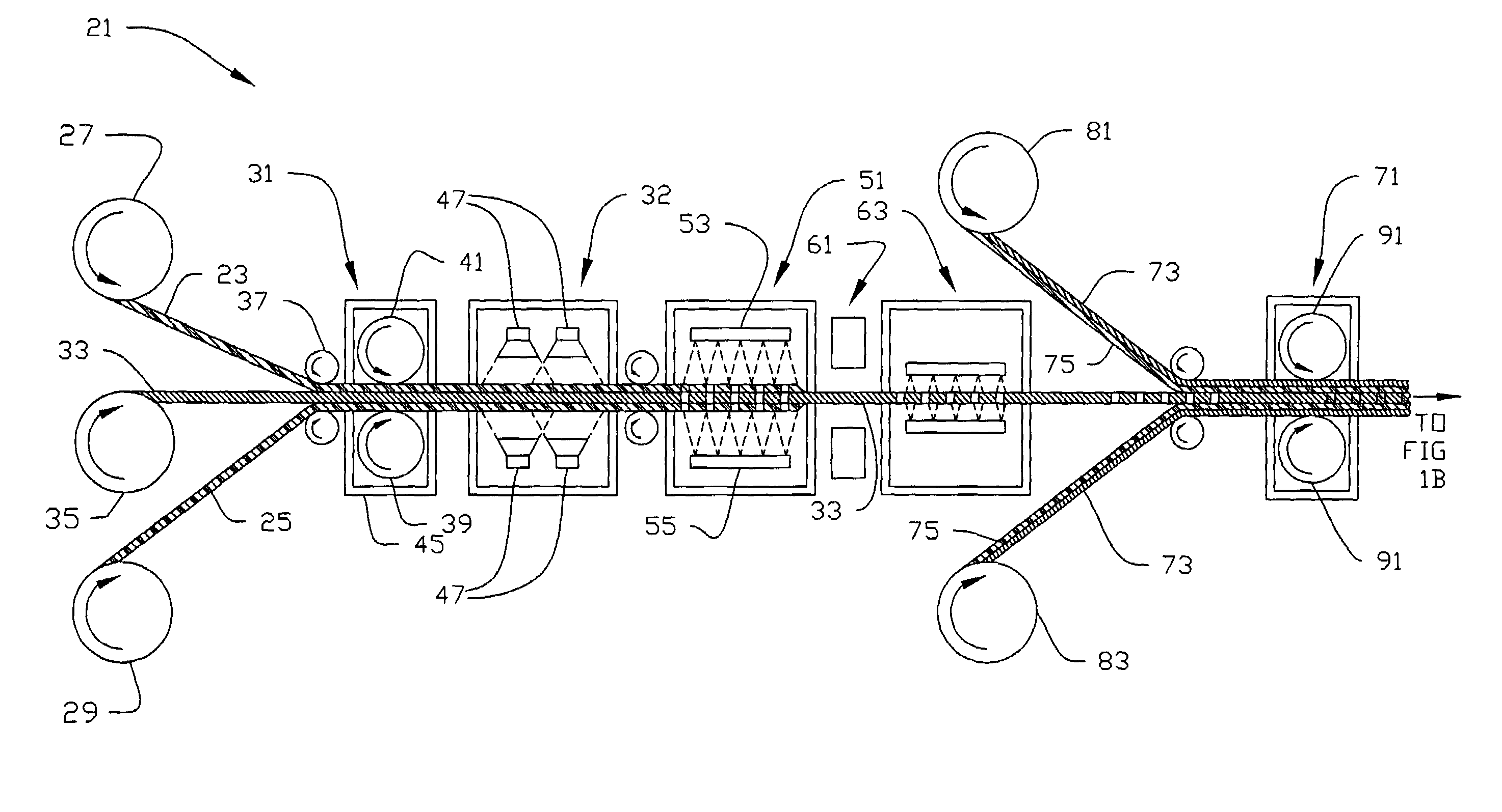
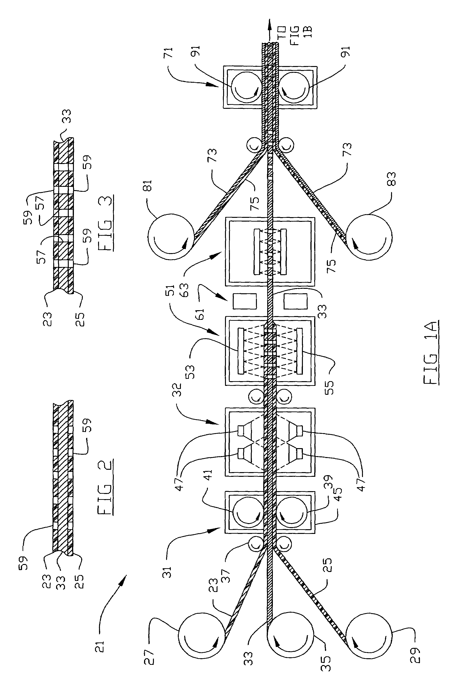
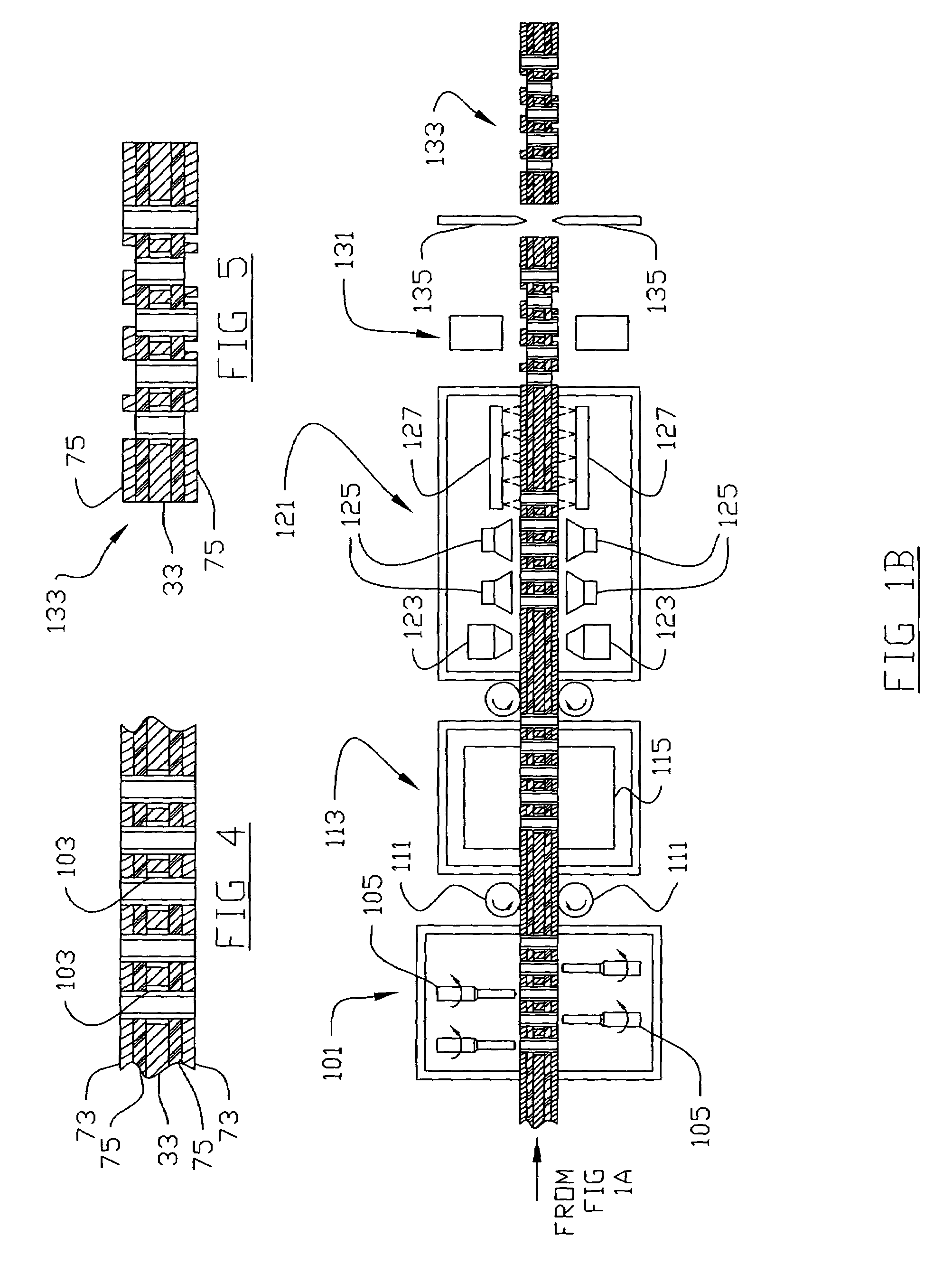
[0047]By the term “continuous” as used herein when defining a process is meant a process in which all of the steps to manufacture a circuitized substrate having at least one conductive layer and two dielectric layers are performed with the at least one conductive layer being in the form of a continuous layer, up to final segmenting to define the final substrate's dimensions. All steps are performed while the conductive layer remains as provided from its original source (e.g., a roll), without segmenting occurring until the last step.

[0048]By the term “circuitized substrate” as used herein is meant to include substrates having at least two (and p...


PUM

PropertyMeasurementUnit
thickaaaaaaaaaa
temperatureaaaaaaaaaa
thicknessaaaaaaaaaa

Abstract

Apparatus and method for making circuitized substrates using a continuous roll format in which layers of conductor and dielectric are fed into the apparatus, bonded, and passed on to other nearby work stations in which various processes such as hole formation, circuitization and, finally, segmentation occur. The resulting substrates can then be individually bonded to other, like substrates to form a larger multi-layered substrate with a plurality of conductive thru-holes, conductive and dielectric layers as part thereof.

Description

TECHNICAL FIELD[0001]This invention relates to the manufacture of circuitized substrates such as printed circuit boards, chip carriers, and the like. The invention particularly relates to the manufacture of such substrates in which conductive thru-holes are provided therein.BACKGROUND OF THE INVENTION[0002]The conventional manufacture of circuitized substrates such as printed circuit boards and chip carriers, especially those of the multi-layered type, involves many individual processes such as etching, plating, lamination, drilling, testing, inspection, etc. Typically, these processes are performed at different locations within the manufacturing facility, requiring shipment of partially completed substrates from one station to another at such different locations. Such transfer is costly and time-consuming, especially when involving multi-layered products, the most common of boards sold today in view of increased operational demands for the products (e.g., computer servers, mainfram...

Claims


Application Information

Patent Timeline
Patent Type & Authority Patents(United States)
IPC IPC(8): H01K3/10
CPCH05K3/44H05K3/445H05K3/462H05K3/4641H05K3/064Y10T29/53204H05K3/427H05K2201/0355H05K2201/09536H05K2201/096H05K2201/10378H05K2203/0143H05K2203/068H05K2203/1545H05K2203/1572Y10T29/49155Y10T29/49126Y10T29/49117Y10T29/53161Y10T29/49165Y10T29/5317H05K3/4069
Inventor LAUFFER, JOHN M.MARKOVICH, VOYA R.ORBAND, JAMES W.WILSON, WILLIAM E.
Owner I3 ELECTRONICS
Why Eureka
Try Eureka