Method of treating conductive layer for use in a circuitized substrate and method of making said substrate having said conductive layer as part thereof

a technology of circuitized substrates and conductive layers, applied in printed circuits, electrical equipment, printed circuit aspects, etc., can solve the problems of only being considered suitable for mechanical polishing, affecting the smoothness of the surface of the substrate, so as to increase the roughness and reduce the cost. , the effect of increasing the roughness

Active Publication Date: 2006-06-08
TTM TECH NORTH AMERICA LLC
View PDF15 Cites 7 Cited by
  • Summary
  • Abstract
  • Description
  • Claims
  • Application Information

AI Technical Summary

Benefits of technology

[0025] It is, therefore, a primary object of the present invention to enhance the circuitized substrate art by providing a method of making a circuitized substrate having one or more conductive layers possessing the advantageous features taught herein.
[0027] It is still another object of the invention to provide such methods which can be accomplished in a relatively facile manner and at relatively low cost in comparison to some known substrate processes.
[0028] According to one aspect of the invention, there is provided a method of treating a conductive layer for use in a circuitized substrate, the method comprising providing a conductive layer of a first metal having at least one smooth side including a first roughness, depositing a layer of a second metal different than the first metal on the smooth side of the conductive layer, exposing the layer of second metal to a solution to reduce the amount of second metal within this layer, and providing a thin polymer layer on the layer of second metal after reducing the second metal, to protect the layer of second metal and to increase the roughness of the conductive layer to a second roughness greater than the first roughness.
[0029] According to another aspect of the invention, there is provided a method of making a circuitized substrate in which the method comprises providing a conductive layer of a first metal having at least one smooth side including a first roughness, depositing a layer of a second metal different than the first metal on the smooth side of the conductive layer, exposing the layer of second metal to a solution to reduce the amount of second metal within this layer, providing a thin polymer layer on the layer of second metal after reducing the second metal, to protect the layer of second metal and to increase the roughness of the conductive layer to a second roughness greater than the first roughness, providing a dielectric layer, bonding the conductive and dielectric layers, and forming a circuit within the conductive layer.

Problems solved by technology

Unfortunately, if the foil is too thin, it may be damaged, e.g., severed or torn in sections, from the relatively high stresses exerted on the copper foil during this processing.
Thus, mechanical polishing is only considered suitable for preparing the surface of relatively thick copper foils.
However, such processes are typically expensive to operate, often requiring relatively expensive equipment, costly chemical baths, as well as prolonged periods during which the foil is so treated, thereby extending the total time of manufacture of the end product.
Such plating may further involve electroplating minor amounts of chromium followed by a thin layer of zinc, this also increasing the roughness.
Such high-speed connections are subjected to various detrimental effects, e.g., signal deterioration (also referred to as signal attenuation), caused by the inherent characteristics of such known substrate circuitry wiring.
Unfortunately, such roughness may also adversely affect signal passage if too excessive.
Moreover, depressed parts are not polished, so that the amount of copper lost by the polishing steps is extremely minute.

Method used


Image

  • Method of treating conductive layer for use in a circuitized substrate and method of making said substrate having said conductive layer as part thereof
  • Method of treating conductive layer for use in a circuitized substrate and method of making said substrate having said conductive layer as part thereof
  • Method of treating conductive layer for use in a circuitized substrate and method of making said substrate having said conductive layer as part thereof

Examples


Embodiment Construction

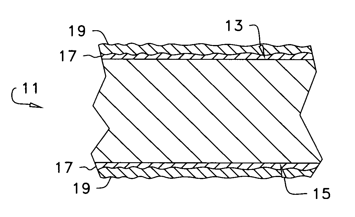
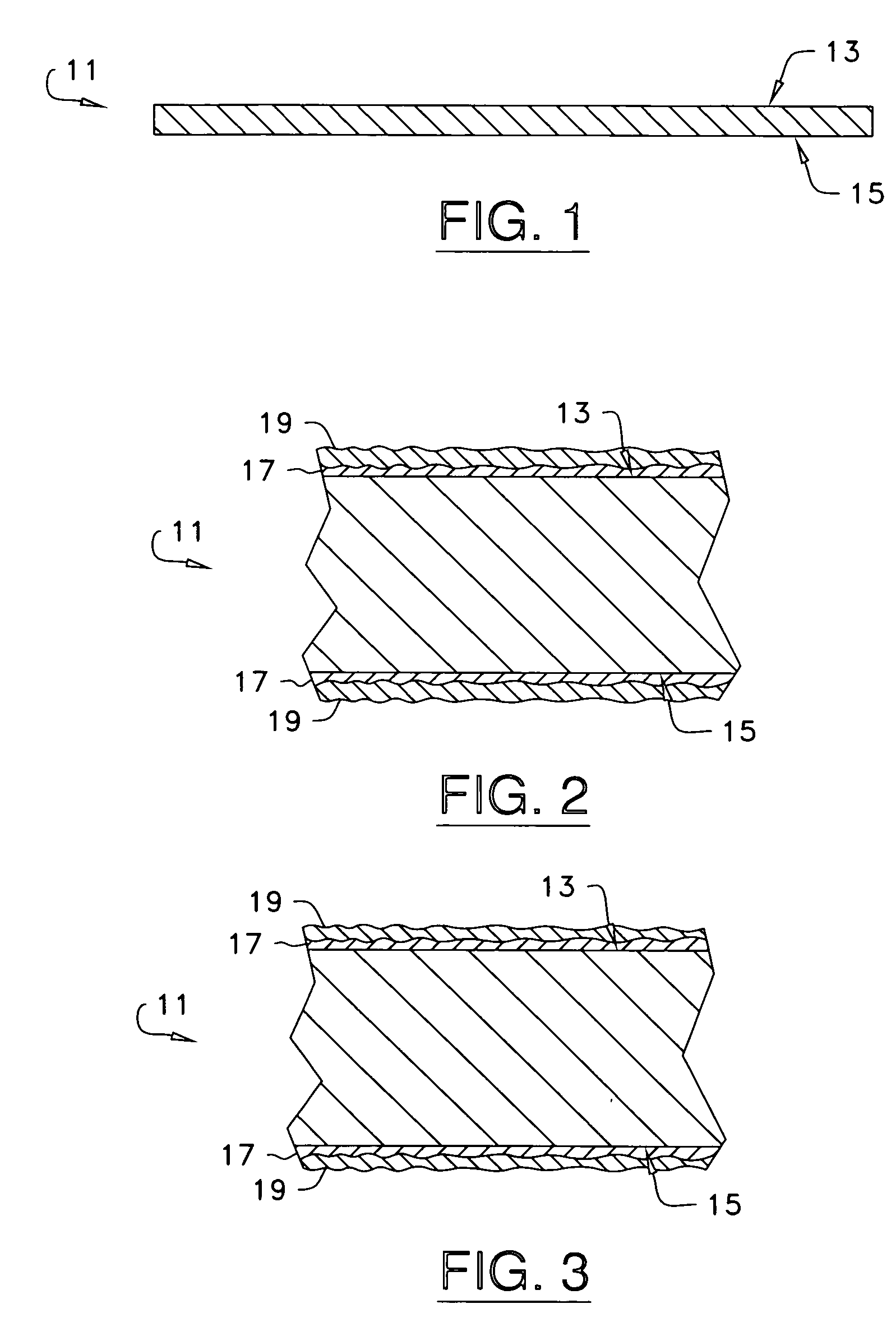
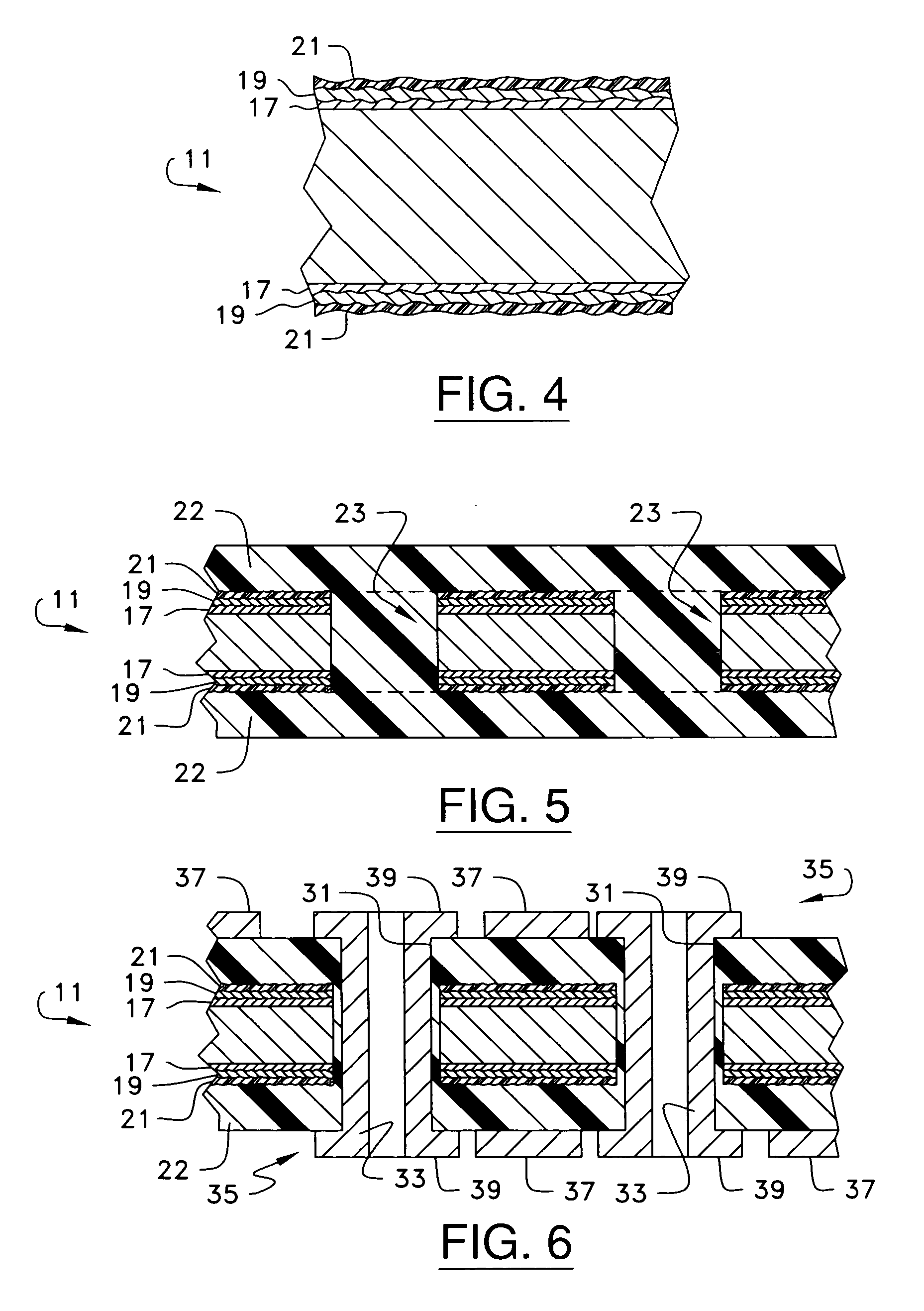
[0034] For a better understanding of the present invention, together with other and further objects, advantages and capabilities thereof, reference is made to the following disclosure and appended claims in connection with the above-described drawings. Like figure numbers will be used from FIG. to FIG. to identify like elements in these drawings.

[0035] By the term “circuitized substrate” as used herein is meant to include substrates having at least one dielectric layer and at least one metal conductive layer. Examples of dielectric materials include fiberglass-reinforced epoxy resins (some referred to as “FR-4” dielectric materials in the art), polytetrafluoroethylene (Teflon), polyimides, polyamides, cyanate resins, polyphenylene ether resins, photoimageable materials, and other like materials wherein the conductive layer(s) is(are) comprised of metal such as copper (preferably electrodeposited copper foil as defined herein-above), and function as a power, signal and / or ground lay...


PUM

PropertyMeasurementUnit
thicknessaaaaaaaaaa
thicknessaaaaaaaaaa
roughnessaaaaaaaaaa

Abstract

A method of treating a conductive layer to assure enhanced adhesion of the layer to selected dielectric layers used to form a circuitized substrate. The conductive layer includes at least one surface with the appropriate roughness to enable such adhesion and also good signal passage if the layer is used as a signal layer. The method is extendible to the formation of such substrates, including to the formation of multilayered substrates having many conductive and dielectric layers. Such substrates may include one or more electrical components (e.g., semiconductor chips) mounted thereon and may also be mounted themselves onto other substrates.

Description

CROSS REFERENCE TO CO-PENDING APPLICATION [0001] In Ser. No. 10 / 991,451, entitled “Circuitized Substrate Utilizing Smooth-Sided Conductive Layers As Part Thereof, Method Of Making Same, And Electrical Assemblies And Information Handling Systems Utilizing Same”, filed Nov. 19, 2004 and assigned to the same Assignee as the present invention, there is defined a substrate in which two conductive layers (e.g., electroplated copper foil) are bonded (e.g., laminated) to an interim dielectric layer. Each of the two foil surfaces which physically bond to the dielectric are smooth (e.g., preferably by chemical processing) and include a thin, organic layer thereon, while the outer surfaces of both foils are also smooth (e.g., preferably also using a chemical processing step). One of these resulting conductive layers may function as a ground or voltage plane while the other may function as a signal plane with a plurality of individual signal lines as part thereof. An electrical assembly and an ...

Claims


Application Information

Patent Timeline
Patent Type & Authority Applications(United States)
IPC IPC(8): H01L21/311C25D5/10H01L21/44
CPCH05K1/056H05K3/384H05K3/386H05K2201/0355H05K2201/0358H05K2203/0353H05K2203/0723
Inventor EGITTO, FRANK D.KRASNIAK, STEPHENLAUFFER, JOHN M.MARKOVICH, VOYA R.MATIENZO, LUIS J.
Owner TTM TECH NORTH AMERICA LLC
Why Eureka
Try Eureka