Charge pump with ensured pumping capability

a technology of shin's pump and discharge pump, which is applied in the field of electronic circuitry, can solve the problems of reducing the power supply voltage range, the vsub>pn /sub>pn is basically not scalable, and the diode pump cannot be readily scaled downward, so as to avoid bipolar action difficulties, reduce the performance of shin's pump, and be easily scaled to small dimensions

Inactive Publication Date: 2007-11-27
MOSEL VITELIC CORP
View PDF11 Cites 26 Cited by
  • Summary
  • Abstract
  • Description
  • Claims
  • Application Information

AI Technical Summary

Benefits of technology

[0025]By having the gate electrode of the second side FET of the first cell coupled to the source of the second clock signal in accordance with the invention, the difference between the voltages at the gate electrode and first S / D region of that FET is greater when it is conductive than what would occur if its gate electrode were, as arises with the gate electrode of the drain-side FET in Shin's first cell, coupled to the input node because the second clock signal is generally inverse to the first clock signal and, during conductive intervals for the second side FET of the first cell in the present charge pump, is at voltage further away from the voltage of the first clock signal than is the pump input voltage. This increased voltage difference prevents the second side FET of the first cell in the charge pump of the invention from turning off when the first clock signal is at the on value for that FET and, accordingly, prevents undesired bipolar action that could cause loss in the stage voltage gain of the first and later pump stages.
[0029]By connecting the gate electrode of the first side FET of the (n+1)th cell in either of the ways described above, the gate electrode of that FET is coupled through one of the capacitive elements to the source of the remaining one of the first and second clock signals. This enables the difference between the voltages at the gate electrode and first S / D region of that FET to be greater when it is conductive than what would occur if its gate electrode were, as arises with the gate electrode of the source-side FET in Shin's (n+1)th cell, coupled to the output node because, during conductive intervals for the first side FET of the (n+1)th cell in the present charge pump, the remaining clock signal is at voltage further away from the voltage of the specified clock signal than is the pump output voltage. This increased voltage difference prevents the first side FET of the (n+1)th cell in the present pump from turning off when the specified clock signal is at the on value for that FET and thereby avoids loss in the pump's overall voltage gain.
[0030]The charge pump of the invention operates as a two-phase device when it is controlled by only two clock signals. The pumping efficiency can be improved by utilizing two more clock signals to create a four-phase implementation. In particular, the present pump can be provided with sources of third and fourth clock signals different from the first and second clock signals. The four clock signals all vary substantially between first and second voltage values. The third clock signal is substantially at the first voltage value during pumping operation only during part of each time interval in which the first clock signal is substantially at the first voltage value. The fourth clock signal is similarly at the first voltage value during pumping operation only during part of each time interval in which the second clock signal is substantially at the first voltage value.
[0033]Coupling the gate electrode of the first side FET of the (n+1)th cell through the additional capacitive element to the source of the selected one of the first and second clock signals in the preceding manner enables the four-phase implementation of the charge pump of the invention to achieve the performance advantages attained by connecting the gate electrode of the (n+1)th cell's first side FET in either of the first two ways described above. That is, the difference between the voltages at the gate electrode and first S / D region of that FET is greater when it is conductive than what would occur if its gate electrode were coupled to the output node. The increased voltage difference again prevents loss in the pump's overall voltage gain.
[0035]In short, the present charge pump avoids bipolar action difficulties that can severely degrade the performance of Shin's pump. At the same time, the pump of the invention achieves an efficiency very close to the efficiency of a diode pump. Since the present pump employs FETs, it can readily be scaled to small dimensions and thereby avoids the scaling difficulties of the diode pump. Consequently, the invention provides a significant advance over the prior art.

Problems solved by technology

However, diode turn-on voltage Vpn is basically not scalable.
As a result, the diode pump cannot be readily scaled downward as the power-supply voltage range is reduced in the course of decreasing the average integrated-circuit feature size.
Also, providing an integrated circuit with pn diodes for a diode pump presents substantial fabrication difficulties.
The stage voltage gain thereby decreases with increasing i. For the same number of stages and same voltage conditions at the first stage, the Dickson pump is less efficient than the diode pump.

Method used


Image

  • Charge pump with ensured pumping capability
  • Charge pump with ensured pumping capability
  • Charge pump with ensured pumping capability

Examples


Embodiment Construction

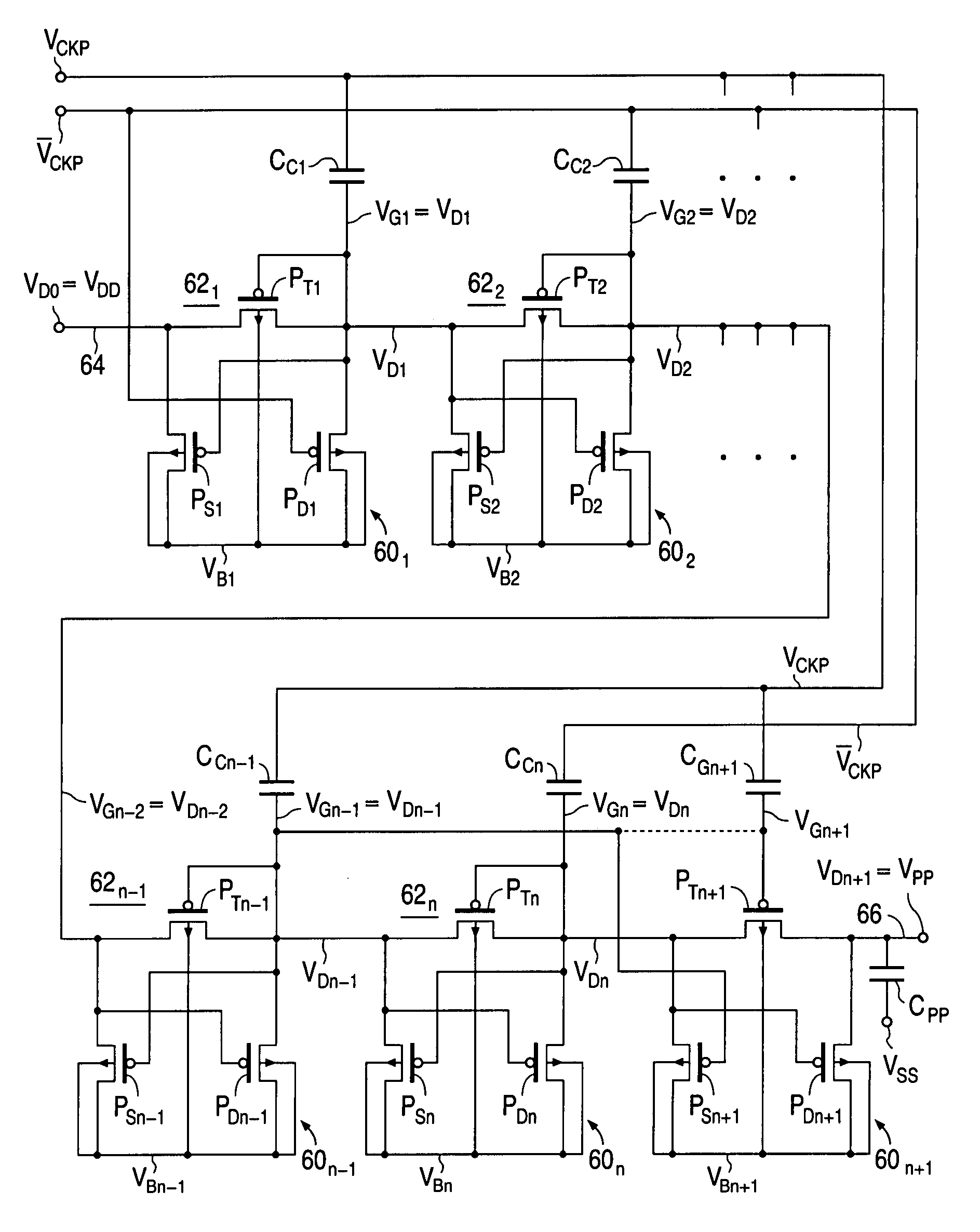
[0052]FIGS. 7a and 7b (collectively “FIG. 7”) illustrate an n-stage two-phase positive charge pump in accordance with the invention. Beginning and end portions of the two-phase positive charge pump are depicted in FIG. 7a. An intermediate pump portion is depicted in FIG. 7b. The charge pump of FIG. 7 operates from a power supply that provides high supply voltage VDD and a low supply voltage VSS, typically ground reference, which define a power-supply voltage range VDD−VSS. High supply voltage VDD is 2.5-4.0 V, typically 3.0 V, when low supply voltage VSS is ground reference.

[0053]The charge pump of FIG. 7 consists of n+1 charge-transfer cells 601, 602, . . . 60n−1, 60n, and 60n+1 arranged in series, n substantially identical primary pump capacitive elements CC1, CC2, . . . CCn−1, and CCn respectively corresponding to charge-transfer cells 601-60n, an additional capacitive element CGn+1, an output capacitive element CPP, and sources (not separately shown) of a first clock voltage sig...


PUM


Abstract

An n-stage charge pump contains n primary capacitive elements (CC1-CCn or CD1-CDn), n+1 charge-transfer cells (601-60n+1, 1101-110n+1, 1201-120n+1, or 1301-130n+1) respectively sequentially designated as the first through (n+1)th cells, and sources of first and second clock signals (VCKP and VCK P or VCKP1 and VCKP2) approximately inverse to each other. Each pump stage (62i, 112i, 122i, or 132i) includes one (CCi or CDi) of the capacitive elements and a corresponding one (60i, 110i, 120i, or 130i) of the first through nth charge-transfer cells. Each cell contains a charge-transfer FET (PTi or NTi). A pair of side FETs (PSi and PDi or NSi and NDi) are provided in the first cell, in the (n+1)th cell, and normally in each remaining cell. The side FETs in the first cell or / and the (n+1) cell are connected in such a manner as to avoid undesired bipolar action that could cause degradation in the pump's voltage gain.

Description

FIELD OF USE[0001]This invention relates to electronic circuitry and, in particular, to charge pumps for use in integrated circuits.BACKGROUND ART[0002]A charge pump is an electronic circuit that uses a pumping technique to generate a pump output voltage outside the range of supply voltages from which the pump operates. When the pump output voltage is greater than the upper limit of the power-supply range, the pump is commonly referred to as a positive charge pump. A charge pump whose output voltage is less than the lower limit of the power-supply range is commonly referred to as a negative charge pump. A charge pump typically contains a group of pump stages arranged in series. Each stage provides an incremental voltage increase or decrease, generally referred to as the stage voltage gain, in the pump output voltage.[0003]FIG. 1 illustrates a conventional n-stage positive diode charge pump whose power-supply range is from ground reference (0 V) to a high voltage denoted here as VDD....

Claims


Application Information

Patent Timeline
Patent Type & Authority Patents(United States)
IPC IPC(8): G05F3/02
CPCG11C5/145
Inventor KIM, JONGJUN
Owner MOSEL VITELIC CORP
Why Eureka
Try Eureka