Amplifier arrangement, and method for compensating for an offset

a compensation method and amplifier technology, applied in the field of amplifier arrangement, can solve the problems of system failure, significant increase of error vectors in digital modulation methods, undesirable effects of direct current (dc) offset, etc., and achieve the effect of improving the operation of the amplifier arrangement, reducing the dc offset at the input of the amplifier, and improving the dc offs

Inactive Publication Date: 2007-12-04
INFINEON TECH AG
View PDF5 Cites 26 Cited by
  • Summary
  • Abstract
  • Description
  • Claims
  • Application Information

AI Technical Summary

Benefits of technology

[0011]In one embodiment of the invention, the amplifier arrangement comprises an amplifier with two inputs and an output, and a feedback path that couples the output to at least one of the two inputs. The arrangement further comprises a first switch configured to couple the two inputs to one another, such that they can be switched in a compensation operating mode, and a second switch configured to interrupt the feedback path in the compensation operating mode. The arrangement also includes a controllable current source coupled to at least one of the two inputs of the amplifier, and a control device configured to couple the output of the amplifier to the controllable current source in order to reduce an offset at the inputs of the amplifier in the compensation operating mode by providing a compensation current.
[0013]In accordance with the invention, DC offsets at the input of the amplifier are compensated for by adding a correction current at the input of the amplifier. In this case, the inputs of the amplifier are connected to one another during calibration or compensation. During the compensation operating mode, the amplifier is operated without an external connection, namely with the feedback path interrupted. This is also referred to as open-loop operation of an amplifier. If there is an offset, the output of the amplifier tilts toward the positive or negative supply voltage of the amplifier, depending on the polarity of the offset. This property is used to determine the suitable compensation signal. A DC offset at the input of the amplifier can thus be avoided or at least considerably reduced.
[0019]If a plurality of amplifiers are provided in a circuit, for example in a transceiver, the compensation operations described can be carried out concurrently, e.g., in parallel, for each operational amplifier. This is made possible by the fact that the inputs of each amplifier are short-circuited in one example and the outputs are disconnected anyway. Adjusting the amplifiers but not the individual programming positions makes it possible to considerably reduce the complexity. Therefore the amplifier itself and not its external connection is evaluated for the offset.
[0028]The compensation in accordance with the invention is accurate enough to significantly improve operation of the amplifier arrangement despite being carried out once, for example when the mobile radio which comprises said amplifier arrangement is switched on. The primary factors of influence for a DC offset are dictated typically by the technology and are dependent on matching of the components and are not primarily caused by temperature and / or drift effects or by supply voltage fluctuations. The DC offset at the input of an amplifier can thus be considerably reduced in accordance with the invention.
[0029]Yet another reduction in the DC offset can be achieved by means of combination with a DC feedback loop of the amplifier arrangement. This makes it possible to increase the compensation accuracy and thus to further reduce its execution speed and implementation complexity. Transients which interfere with the system are nevertheless reduced to a negligible level.
[0030]According to one or more aspects of the present invention, the control circuit comprises a signal input for disconnection. This signal input is connected to the circuit, with the circuit in the active operating state being designed to output a disconnection signal to the control circuit. This reduces the power consumption of the control circuit, since said control circuit is no longer required during the active operating state.

Problems solved by technology

Such direct current (DC) offsets may have undesirable effects in transmission arrangements, for example.
This significantly increases error vectors in digital modulation methods.
In the reception path of a mobile radio, a DC offset may even result in system failure since the extremely high gain in the analog baseband may result in transient spikes which may drive individual stages of the signal processing chain into saturation and may result in analog / digital converters being overdriven.
However, such AC coupling requires a relatively large chip area on account of the series capacitances which are normally provided for implementation.
In addition, information components of useful information may be removed or filtered out in an undesirable manner.
Accordingly, it is not possible, in contrast to earlier mobile radio methods, for example GSM (Global System for Mobile Communication), which operate using time division multiple access, to periodically interrupt the signal chain in order to be able to carry out calibrations during transmission operation.
However, this principle has the disadvantage that a relatively low cut-off frequency of the high-pass filter is required in order to avoid the useful signal being excessively distorted.
However, this means that the transient response time becomes relatively long, which, in turn, has adverse effects on the received signal.
Another disadvantage results from transients which may occur when there is a sudden change in the gain, even in the case of high-pass filters which settle more rapidly, and may exceed the useful signal many times over.
The analog / digital converter thus cannot be controlled in an ideal manner.
In particular, the switching transients which have been mentioned and occur when the gain value is changed in the reception path of a transmission / reception unit result in considerably impaired electrical properties of the receiver.

Method used


Image

  • Amplifier arrangement, and method for compensating for an offset
  • Amplifier arrangement, and method for compensating for an offset
  • Amplifier arrangement, and method for compensating for an offset

Examples


Embodiment Construction

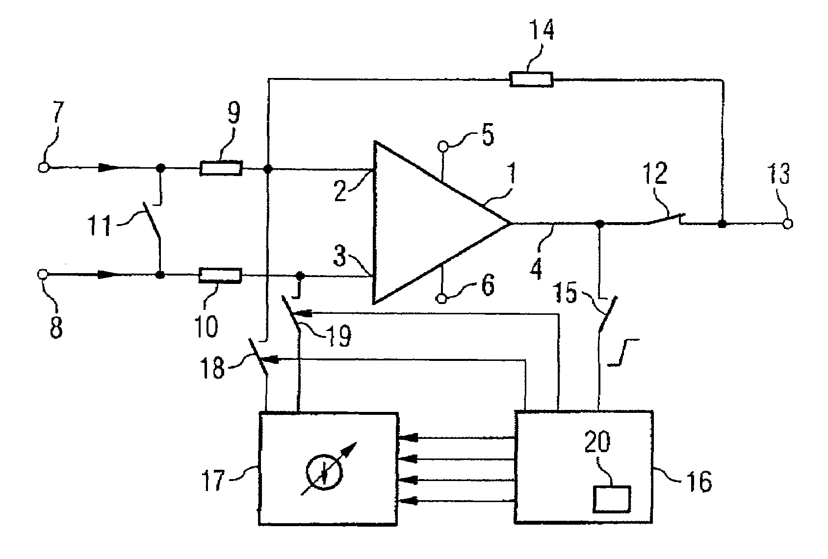
[0039]FIG. 1 shows an operational amplifier 1 having a first input 2, a second input 3 and an output 4. In addition, provision is made of respective connections 5, 6 for supplying a supply potential and a reference potential for the operational amplifier 1. A differential input 7, 8 of the arrangement is coupled to the inputs 2, 3 of the operational amplifier via a respective resistor 9, 10. A switch 11 which is in the form of a normally open contact is connected between the terminals 7, 8 of the differential input in order to selectively short-circuit the inputs 2, 3 of the operational amplifier in a compensation operating mode of the operational amplifier. In this case, the inputs 2, 3 are connected to one another via the series circuit comprising the resistors 9, 10. The output 4 of the operational amplifier is coupled selectively to an output 13 of the amplifier arrangement via a switch 12 which is in the form of a normally closed contact.

[0040]The output 13 of the arrangement i...


PUM


Abstract

An amplifier arrangement and a method for compensating for an offset in an amplifier is provided. A respective switch for connecting together the inputs in a compensation operating mode and for interrupting the feedback path in this operating mode is provided in an amplifier. A control device detects an output signal and drives a controllable current source, which can be coupled to one of the two inputs of the amplifier, in such a manner that a compensation current which minimizes the offset is provided. The arrangement and method can be used, for example, in transmission arrangements.

Description

REFERENCE TO RELATED APPLICATIONS[0001]This application claims the benefit of the priority date of German application DE 10 2005 007 632.7, filed on Feb. 18, 2005, the contents of which are herein incorporated by reference in their entirety.FIELD OF THE INVENTION[0002]The present invention relates to an amplifier arrangement, to the use thereof, and to a method for compensating for an offset in an amplifier.BACKGROUND OF THE INVENTION[0003]Offsets may have different causes in a signal processing chain of an integrated circuit. Fluctuations in the supply voltage, temperature drift effects, fluctuations in process parameters during fabrication and matching problems between electronic components in the case of differential signal routing thus contribute, for example, to the occurrence of offsets.[0004]Such direct current (DC) offsets may have undesirable effects in transmission arrangements, for example. DC offsets which occur in the baseband signal processing system of a transmitter t...

Claims


Application Information

Patent Timeline
Patent Type & Authority Patents(United States)
IPC IPC(8): H03F1/02
CPCH03F1/34H03F3/24H03F3/45977H03F3/45968H03F3/45475
Inventor KOLLER, RAINERWAGENLEITNER, THOMASMUTLU, VAROL
Owner INFINEON TECH AG
Why Eureka
Try Eureka