Auto-zero circuit

a technology of auto-zero circuit and amplifier, which is applied in the direction of pulse automatic control, digital transmission, amplifier with semiconductor devices/discharge tubes, etc., can solve the problems of insufficient voltage capabilities in such new processes for high dynamic range applications, offset errors resulting from finite gain of amplifier, and adversely affecting the operation of feed-forward amplifiers. , to achieve the effect of reducing the noise of the amplifier, reducing the error of charge injection, and reducing the error of auto

Active Publication Date: 2006-09-07
CADENCE DESIGN SYST INC
View PDF2 Cites 26 Cited by
  • Summary
  • Abstract
  • Description
  • Claims
  • Application Information

AI Technical Summary

Benefits of technology

[0016] The accuracy of an auto-zero circuit is limited by the charge injection of the switches, the finite gain limitations, and the noises of the amplifier. A multi-phase approach is used to reduce the charge injection error, the finite gain limitations, and the noises of the amplifier. The first phase operates as a basic correction step for correcting the inherent offset of the amplifier; the second phase is capacitive attenuated to divide down the charge injection error due to sampling of its switches; and the third stage corrects the finite gain error resulting from the second stage operation and further reduces the offset due to charge injection. The bandwidth of the second and third stage operation is reduced to the minimum needed for the amplifier output signal to settle in the allowed time and to limit the noise bandwidth to the minimum possible.
[0018] In another embodiment, a method for performing offset adjustment of an auto-zero circuit includes correcting an inherent offset of the auto-zero circuit by a first set of circuits in a first auto-zero phase and reducing charge injection error and noise error of the auto-zero circuit by a second set of circuits in a second auto-zero phase. The first set of circuits includes a first differential amplifier and a first feedback path coupled between an output of the first differential amplifier and an input of the first differential amplifier. The second set of circuits includes a second differential amplifier and a second feedback path coupled between an output of the second differential amplifier and an input of the first differential amplifier, where the second feedback path includes an attenuation capacitor and a holding capacitor.

Problems solved by technology

These sidebands can adversely impact the operation of the feed-forward amplifier when the input frequency is very close to the auto-zero frequency and the side band appears at or around the frequency of direct current (DC).
There are a number of issues with the circuit of FIG. 1b.
In newer processes, the charge injection may drop to as low as 0.25 fC, but the voltage capabilities in such new processes tend not to be adequate for the high dynamic range applications.
In addition, there is an offset error resulting from the finite gain of the amplifier.
This is not practical for most applications.
Furthermore, there is broadband noise that is aliased down to baseband from the sampling operation.
One is the noise of the amplifier in the total bandwidth of the auto-zero loop when it is brought down to baseband.
The use of newer deep sub-micron processes makes this possible, although this approach is expensive because of the large chip area and the advanced process technology employed.
As discussed above, the prior art solutions require large on-chip area, external components, or expensive newer processing technology.
All such solutions lead to higher product costs.
The accuracy of an auto-zero circuit is limited by the charge injection of the switches, the finite gain limitations, and the noises of the amplifier.

Method used


Image

  • Auto-zero circuit
  • Auto-zero circuit
  • Auto-zero circuit

Examples


Embodiment Construction

[0025] Various embodiments of auto-zero circuits are described and methods are provided for performing offset adjustment of an auto-zero circuit. The following descriptions are presented to enable any person skilled in the art to make and use the invention. Descriptions of specific embodiments and applications are provided only as examples. Various modifications and combinations of the examples described herein will be readily apparent to those skilled in the art, and the general principles defined herein may be applied to other examples and applications without departing from the spirit and scope of the invention. Thus, the present invention is not intended to be limited to the examples described and shown, but is to be accorded the widest scope consistent with the principles and features disclosed herein.

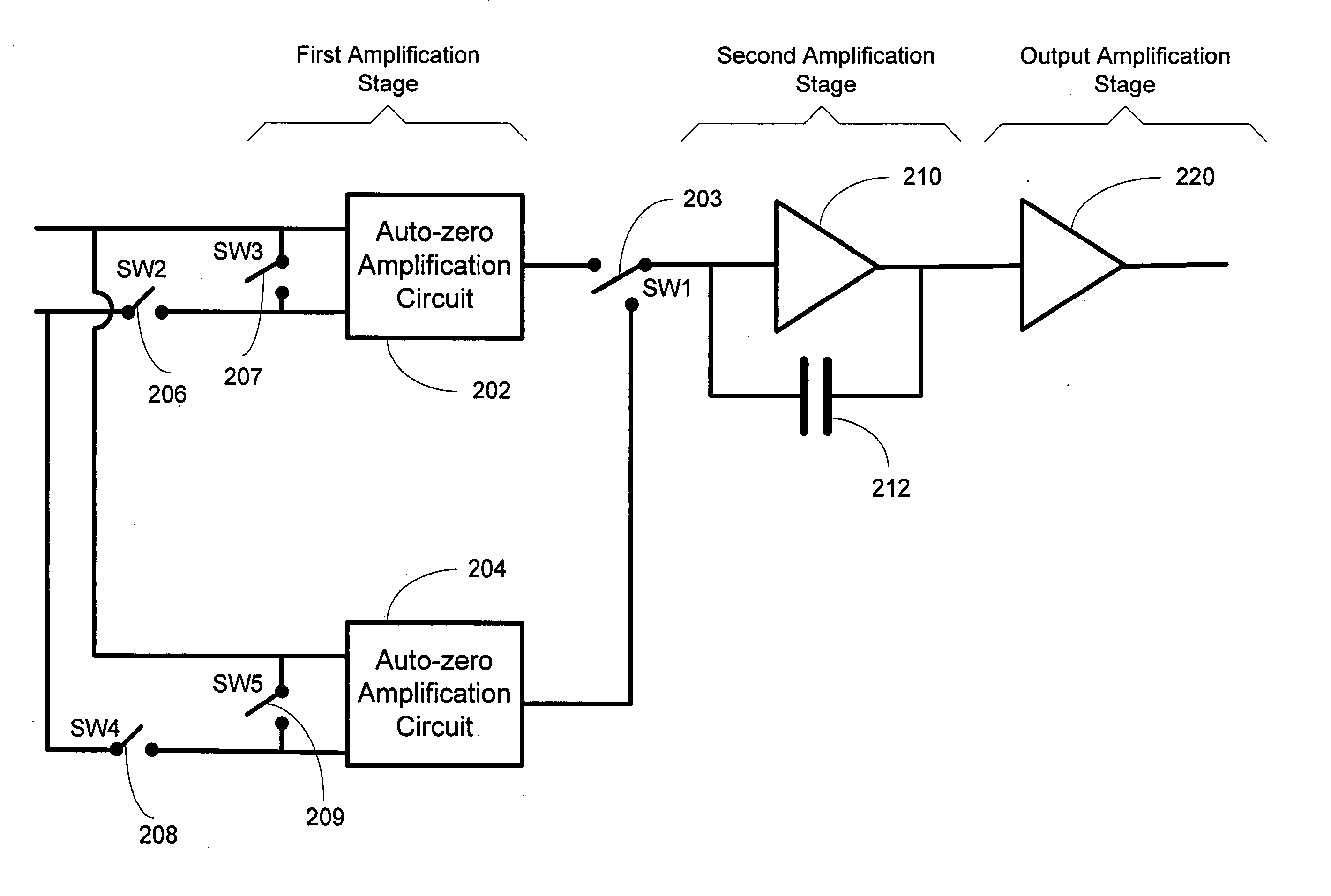
[0026]FIG. 2 illustrates a block diagram of a ping-pong architecture where an auto-zero circuit is used according to an embodiment of the present invention. As shown in FIG. 2, t...


PUM


Abstract

An auto-zero circuit is disclosed. The auto-zero circuit includes a first set of circuits for implementing a first auto-zero phase and a second set of circuits for implementing a second auto-zero phase. The first set of circuits includes a first differential amplifier and a first feedback path coupled between an output of the first differential amplifier and an input of the first differential amplifier. The second set of circuits includes a second differential amplifier and a second feedback path coupled between an output of the second differential amplifier and an input of the first differential amplifier, where the second feedback path includes an attenuation capacitor for reducing charge injection error and noise error of the auto-zero circuit and a holding capacitor for holding a voltage to be used to correct charge injection error introduced by the first feedback path.

Description

FIELD OF THE INVENTION [0001] The present invention relates to the field of analog integrated circuit design. In particular, the present invention relates to an auto-zero circuit. BACKGROUND OF THE INVENTION [0002] The inherent offset of an integrated amplifier is on the order of millivolts (mV). To process baseband signals in the microvolt (μV) or less region, a means of reducing the offset of the amplifier is required. It is also desirable to reduce the level of the low frequency noise without using large input transistors. One method for correcting the inherent offset is shown in FIG. 1. [0003]FIG. 1a illustrates a prior art feed-forward amplifier for correcting the inherent offset of the amplifier. The feed-forward amplifier includes a main differential amplifier 102, an auxiliary amplifier 103, a second stage amplifier 104 and its compensation capacitor 105, and an output amplifier 106. The main differential amplifier 102 has two sets of inputs. The first set of inputs is 110, ...

Claims


Application Information

Patent Timeline
Patent Type & Authority Applications(United States)
IPC IPC(8): H03L5/00
CPCH03F3/45475H03F3/45973
Inventor NAVIASKY, ERICBROWN, JIM
Owner CADENCE DESIGN SYST INC
Why Eureka
Try Eureka