Measuring threshold voltage distribution in memory using an aggregate characteristic

a threshold voltage and aggregate characteristic technology, applied in the field of memory devices, can solve the problems of traditional approaches to computing threshold voltage distribution, read errors can occur, voltage distribution of a set, etc., and achieve the effect of reducing read errors in a memory and reducing read errors

Active Publication Date: 2008-11-20
SANDISK CORP +1
View PDF39 Cites 242 Cited by
  • Summary
  • Abstract
  • Description
  • Claims
  • Application Information

AI Technical Summary

Benefits of technology

[0014]The present invention provides a method and apparatus for reducing read errors in a memory. In one aspect, read errors are reduced by determining a threshold voltage distribution of a set of storage elements based on a combined current or other aggregate characteristic of the set. Based on the threshold voltage distribution, optimal read reference voltages can be set for reading the set of storage elements.

Problems solved by technology

However, the read reference voltages are typically fixed and do not account for the fact that the threshold voltage distribution of a set of storage elements can change, e.g., due to factors such as charge leakage, temperature changes, number of programming cycles and the like.
As a result, read errors can occur.
However, traditional approaches for computing threshold voltage distribution, e.g., using external analog equipment or the like, lack flexibility and efficiency for being implemented “on-line” in real time flash management procedures or manufacturing testing, for instance, where the time element is critical.

Method used


Image

  • Measuring threshold voltage distribution in memory using an aggregate characteristic
  • Measuring threshold voltage distribution in memory using an aggregate characteristic
  • Measuring threshold voltage distribution in memory using an aggregate characteristic

Examples


Embodiment Construction

[0049]The present invention provides a method and apparatus for reducing read errors in a non-volatile storage system.

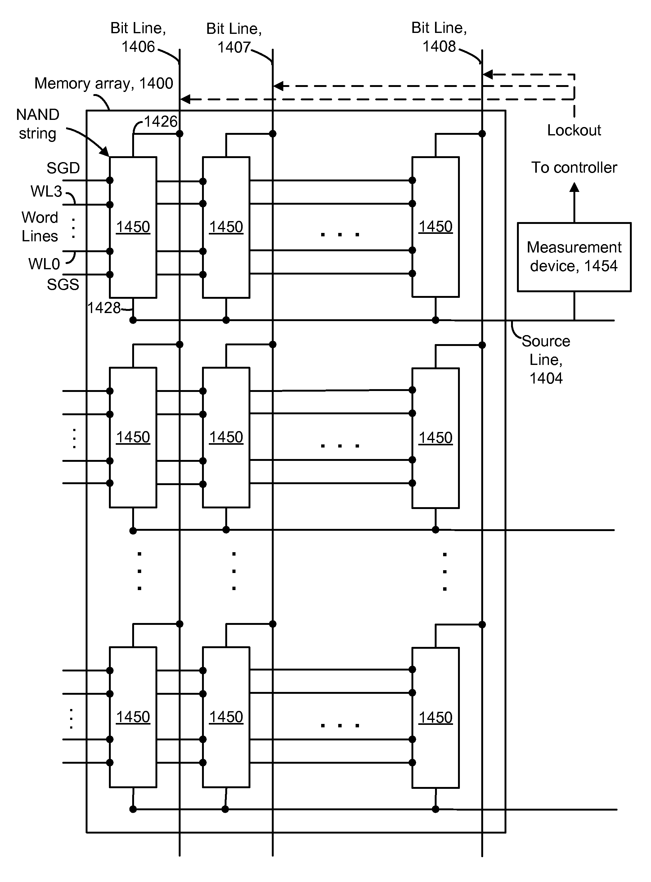
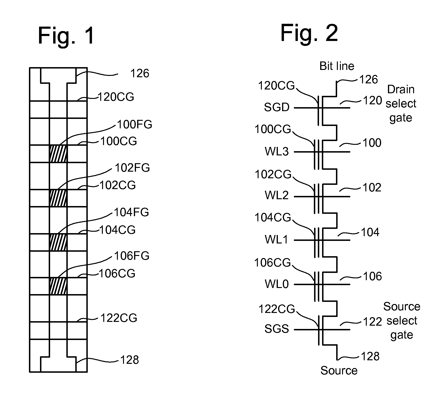
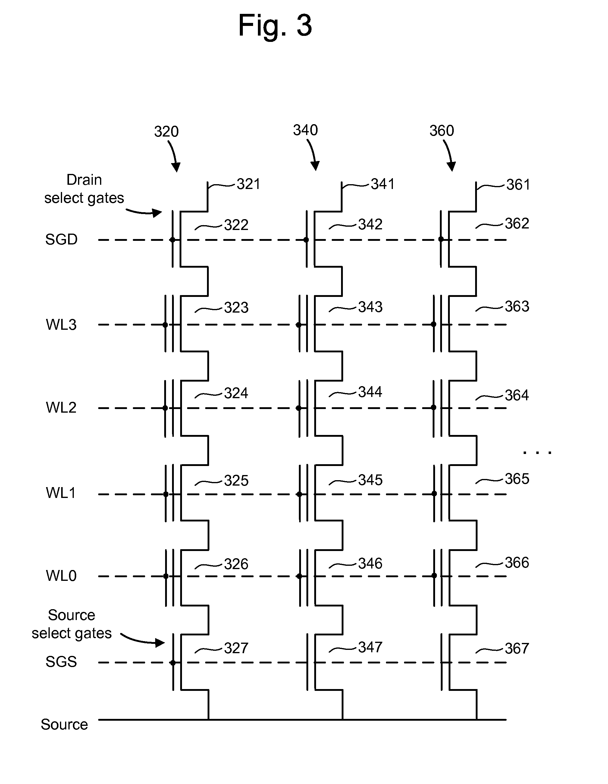
[0050]One example of a memory system suitable for implementing the present invention uses the NAND flash memory structure, which includes arranging multiple transistors in series between two select gates. The transistors in series and the select gates are referred to as a NAND string. FIG. 1 is a top view showing one NAND string. FIG. 2 is an equivalent circuit thereof. The NAND string depicted in FIGS. 1 and 2 includes four transistors, 100, 102, 104 and 106, in series and sandwiched between a first select gate 120 and a second select gate 122. Select gate 120 gates the NAND string connection to bit line 126. Select gate 122 gates the NAND string connection to source line 128. Select gate 120 is controlled by applying the appropriate voltages to control gate 120CG. Select gate 122 is controlled by applying the appropriate voltages to control gate 122CG. Each of the ...


PUM


Abstract

A threshold voltage distribution of a set of storage elements in a memory device is measured by sweeping a control gate voltage while measuring a characteristic of the set of storage elements as a whole. The characteristic indicates how many of the storage elements meet a given condition, such as being in a conductive state. For example, the characteristic may be a combined current, voltage or capacitance of the set which is measured at a common source of the set. The control gate voltage can be generated internally within a memory die. Similarly, the threshold voltage distribution can be determined internally within the memory die. Optionally, storage elements which become conductive can be locked out, such as by changing a bit line voltage, so they no longer contribute to the characteristic. New read reference voltages are determined based on the threshold voltage distribution to reduce errors in future read operations.

Description

CROSS REFERENCE TO RELATED APPLICATIONS[0001]This application claims the benefit of U.S. provisional patent application No. 60 / 917,679, filed on May 14, 2007, and incorporated herein by reference.[0002]This application is related to co-pending, commonly assigned U.S. patent application no. ______, titled “Operating Sequence And Commands For Measuring Threshold Voltage Distribution In Memory” (docket no. SAND-1282US0 / MSD-0023), filed herewith and incorporated herein by reference.BACKGROUND OF THE INVENTION[0003]1. Field of the Invention[0004]The present invention relates to a memory device.[0005]2. Description of the Related Art[0006]Semiconductor memory has become increasingly popular for use in various electronic devices. For example, non-volatile semiconductor memory is used in cellular telephones, digital cameras, personal digital assistants, mobile computing devices, non-mobile computing devices and other devices. Electrically Erasable Programmable Read Only Memory (EEPROM) and ...

Claims


Application Information

Patent Timeline
Patent Type & Authority Applications(United States)
IPC IPC(8): G11C16/04G11C7/00
CPCG11C11/5621G11C16/04G11C16/0483G11C16/3418G11C29/02G11C29/021G11C29/028G11C29/50G11C29/50004G11C2211/5634G11C16/34G11C16/08G11C16/30
Inventor SHLICK, MARKLASSER, MENAHEM
Owner SANDISK CORP
Why Eureka
Try Eureka