Phase change memory devices having phase change area in porous dielectric layer

a phase change memory and dielectric layer technology, applied in the field of memory devices, can solve the problems of affecting the speed of the device, difficult to reduce the area of the lower electrode below a certain level, etc., and achieve the effect of reducing or minimizing a phase change area, and reducing or minimizing the phase change area

Active Publication Date: 2008-01-29
SAMSUNG ELECTRONICS CO LTD
View PDF31 Cites 151 Cited by
  • Summary
  • Abstract
  • Description
  • Claims
  • Application Information

AI Technical Summary

Benefits of technology

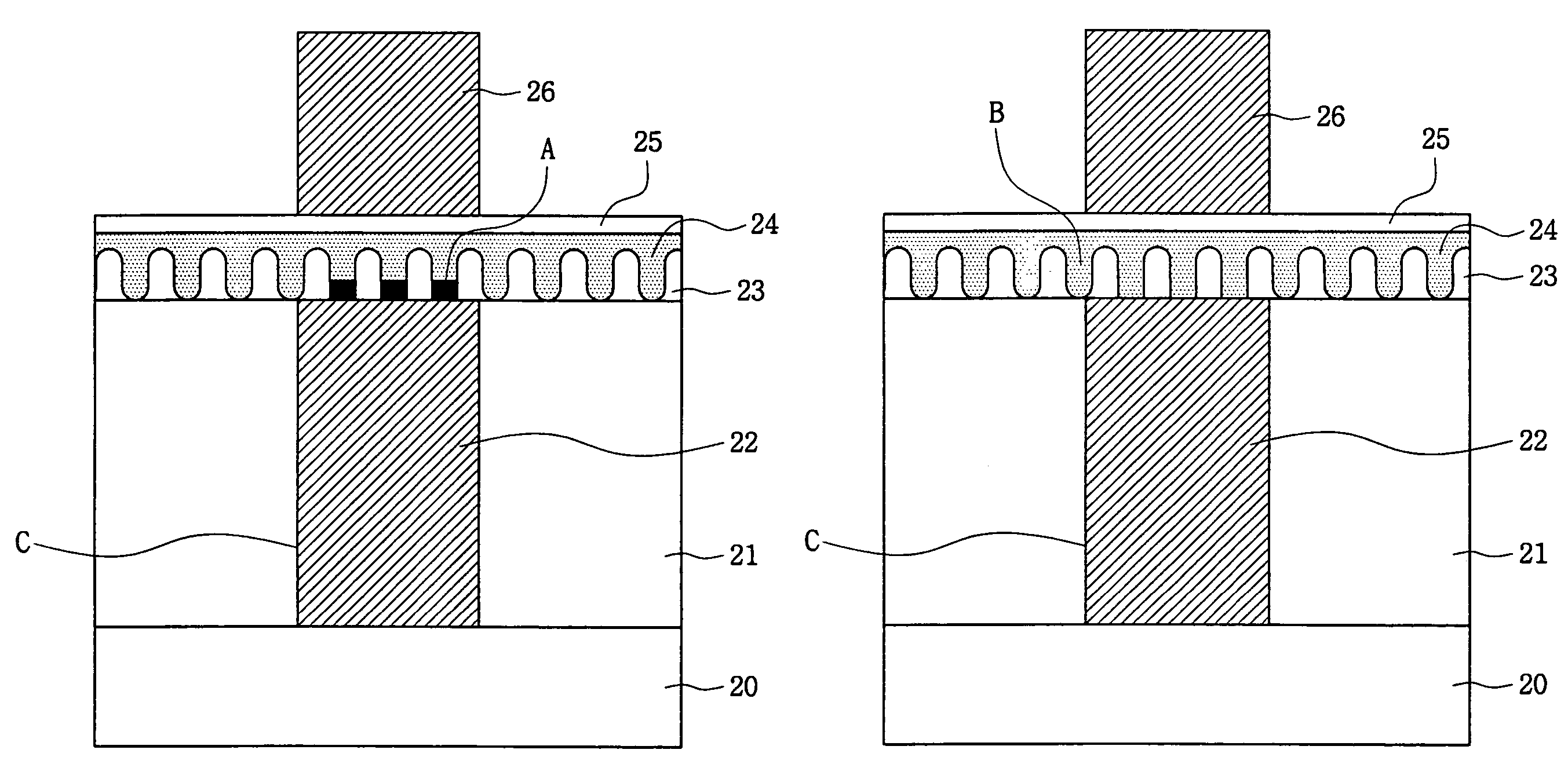
[0017]Some embodiments of the present invention can reduce or minimize a phase change area by forming an absenced pattern phase change layer such as a porous dielectric layer having a plurality of fine pores on the lower electrode, and forming the phase change layer in the fine pores in the porous dielectric layer. As such, a reduced or minimized phase change area may be formed, so that a programming current can be reduced and a crystallization time can be shortened.

Problems solved by technology

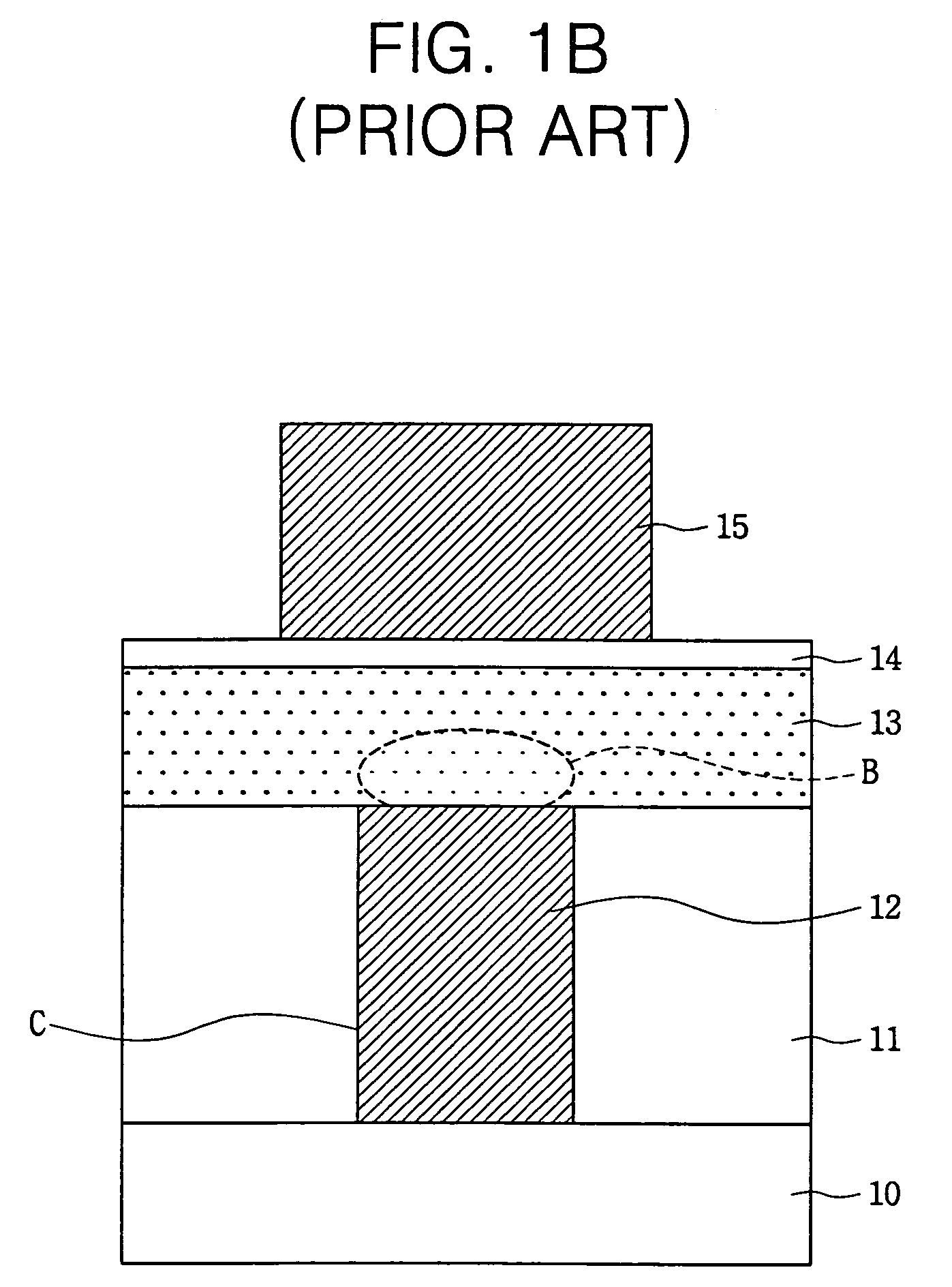
Moreover, it may take hundreds of nanoseconds to several microseconds for the conventional phase change memory device to crystallize an amorphous region, which may affect the speed of the device.
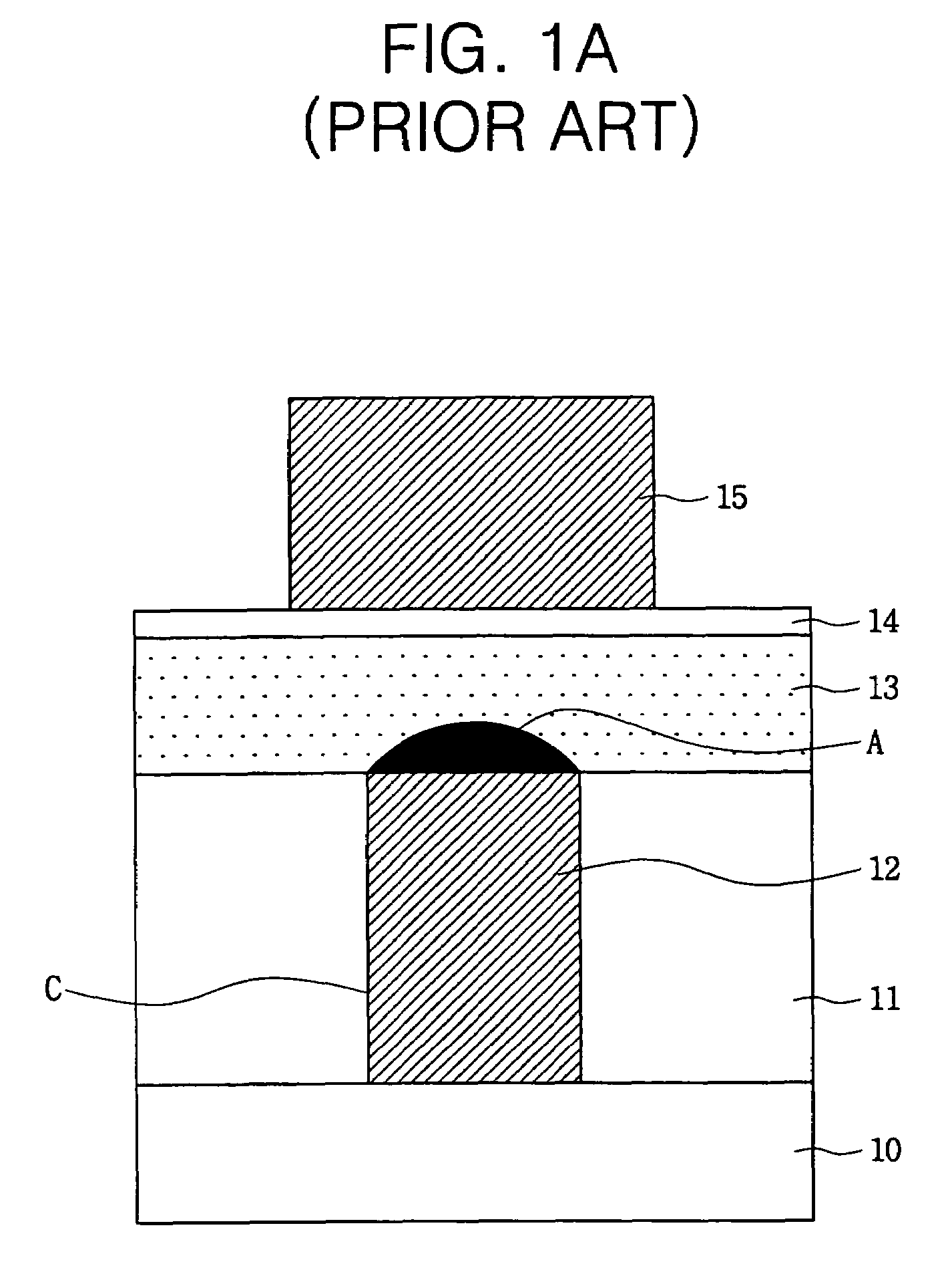
However, a size of a contact hole C that determines the contact area between the lower electrode 12 and the phase change layer 13 generally depends on a photolithography process, and it may be difficult to reduce the area of the lower electrode below a certain level.

Method used


Image

  • Phase change memory devices having phase change area in porous dielectric layer
  • Phase change memory devices having phase change area in porous dielectric layer
  • Phase change memory devices having phase change area in porous dielectric layer

Examples


Embodiment Construction

[0025]The present invention now will be described more fully hereinafter with reference to the accompanying drawings, in which embodiments of the invention are shown. This invention may, however, be embodied in many different forms and should not be construed as limited to the embodiments set forth herein. Rather, these embodiments are provided so that this disclosure will be thorough and complete, and will fully convey the scope of the invention to those skilled in the art. In the drawings, the size and relative sizes of layers and regions may be exaggerated for clarity. Like numbers refer to like elements throughout.

[0026]It will also be understood that when an element such as a layer, region or substrate is referred to as being “on” another element, it can be directly on the other element or intervening elements may also be present. Furthermore, relative terms such as “lower” or “upper” may be used herein to describe a relationship of one layer or region to another layer or regio...


PUM

PropertyMeasurementUnit
diameteraaaaaaaaaa
temperatureaaaaaaaaaa
phase changeaaaaaaaaaa

Abstract

A phase change memory device includes a lower electrode and a porous dielectric layer having fine pores on the lower electrode. A phase change layer is provided in the fine pores of the porous dielectric layer. An upper electrode is provided on the phase change layer. Related manufacturing methods are also described.

Description

RELATED APPLICATION[0001]This application claims the benefit of Korean Patent Application No. 2003-50779, filed on Jul. 23, 2003, the disclosure of which is hereby incorporated herein by reference in its entirety as if set forth fully herein.BACKGROUND OF THE INVENTION[0002]1. Field of the Invention[0003]The present invention relates to memory devices and methods for manufacturing the same and, more particularly, to phase change memory devices and methods for manufacturing the same.[0004]2. Description of the Related Art[0005]Electrically writable and erasable phase change materials are used in semiconductor memory devices. The phase change material can be electrically switched by a change between an amorphous state and a crystal state. See, for example, U.S. Pat. Nos. 3,271,591 and 3,530,441 to Ovshinsky. The phase change material can be switched in an incremental step, reflecting a change of a localized order, in order to provide a “gray scale” represented by various conditions of...

Claims


Application Information

Patent Timeline
Patent Type & Authority Patents(United States)
IPC IPC(8): H01L29/04H01L29/00H01L29/02H01L29/06H01L47/00H01L27/10H01L45/00
CPCH01L45/06H01L45/1233H01L45/1246H01L45/144H01L45/1683H10N70/828H10N70/231H10N70/066H10N70/8828H10N70/826H01L27/10
Inventor LEE, SE-HOHWANG, YOUNG-NAM
Owner SAMSUNG ELECTRONICS CO LTD
Why Eureka
Try Eureka