Substrates adapted for adhesive bonding

a technology of substrates and adhesives, applied in the field of substrates, can solve the problems of affecting the adhesion bonding performance of substrates, affecting the adhesion performance of substrates, and general inability to abrade substrate surfaces,

Inactive Publication Date: 2008-03-11
MEMJET TECH LTD
View PDF14 Cites 2 Cited by
  • Summary
  • Abstract
  • Description
  • Claims
  • Application Information

AI Technical Summary

Benefits of technology

[0033]The invention is particularly advantageous for use in fabrication of printhead chips, because printhead chips typically have ink supply channels etched into a backside bonding surface. Therefore, the trenches of the present invention may be etched at the same time as the ink supply channels, without requiring any additional steps in the fabrication process.
[0036]The trenches may have any depth suitable for improving adhesion without compromising the overall robustness of the first substrate. Optionally, the trenches are etched to depth of at least 10 μm, optionally at least 20 μm, optionally at least 30 μm, or optionally at least 50 μm. Typically, the trenches have an aspect ratio of at least 3:1, at least 5:1 or at least 10:1. High aspect ratio trenches may be readily etched by any known anisotropic etching technique (e.g. the Bosch process described in U.S. Pat. No. 5,501,893). High aspect ratios are advantageous for maximizing the available surface area for the adhesive, without compromising on overall mechanical strength.

Problems solved by technology

However, when bonding microscale substrates, such as semiconductor integrated circuits (“chips”), it is generally not desirable to abrade a surface of the substrate.
Any defects on the surface of the integrated circuit can result in crack propagation and significantly weaken the device.
Moreover, mechanical grinding can result in defects (e.g. cracks or dislocations), which extend up to about 20 μm into the back surface of the wafer.
In terms of mechanical strength, surface roughness and surface defects are unacceptable in integrated circuits.
However, it will be appreciated that integrated circuits have contradictory requirements of their backside surfaces.

Method used


Image

  • Substrates adapted for adhesive bonding
  • Substrates adapted for adhesive bonding
  • Substrates adapted for adhesive bonding

Examples


Embodiment Construction

[0117]A specific form of the invention is described below in the context of fabricating a printhead assembly for an inkjet printer. However, it will be appreciated that the invention may be used in connection with bonding any two substrates together and is not in any way limited to the specific embodiment of printhead fabrication.

Inkjet Printer Unit

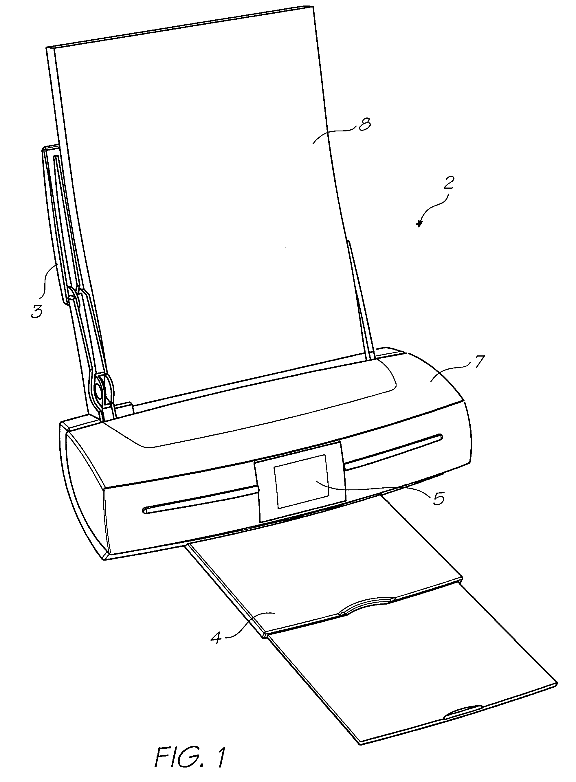
[0118]FIG. 1 shows a printer unit 2 comprising a media supply tray 3, which supports and supplies media 8 to be printed by the print engine (concealed within the printer casing). Printed sheets of media 8 are fed from the print engine to a media output tray 4 for collection. User interface 5 is an LCD touch screen and enables a user to control the operation of the printer unit 2.

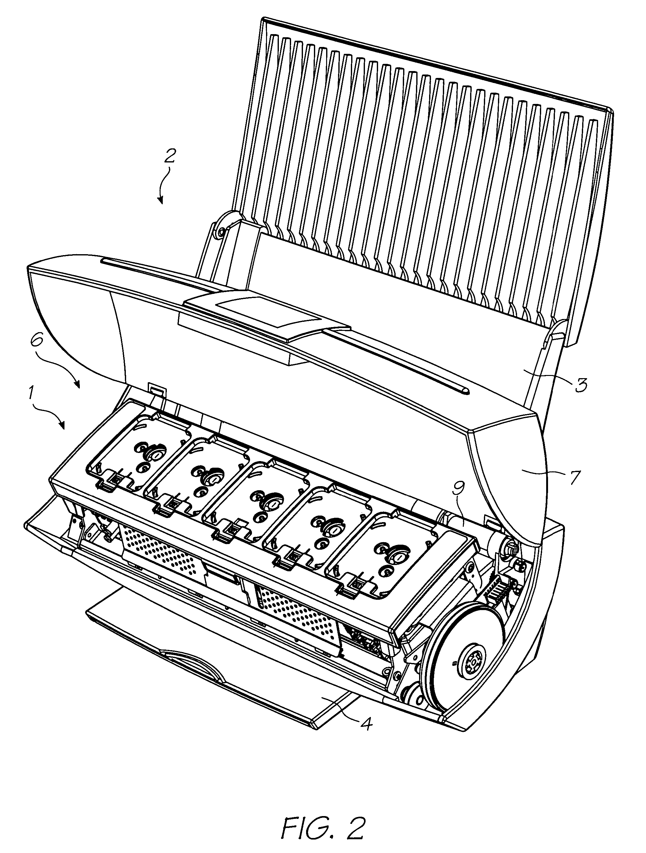
[0119]FIG. 2 shows the lid 7 of the printer unit 2 open to expose the print engine 1 positioned in the internal cavity 6. Picker mechanism 9 engages the media in the input tray 3 (not shown for clarity) and feeds individual streets to the print engine 1. The print...


PUM


Abstract

A first substrate suitable for bonding to a second substrate using an adhesive is provided. The first substrate has a plurality of etched trenches defined in a first bonding surface. The etched trenches are configured for receiving the adhesive during bonding, thereby increasing the adhesive bond strength. The first substrates are exemplified by semiconductor chips.

Description

FIELD OF THE INVENTION[0001]This invention relates to a method of bonding substrates together and a substrate adapted therefore. It has been developed primarily for maximizing bonding of microscale substrates to other substrates, whilst avoiding traditional surface abrasion techniques.CO-PENDING APPLICATIONSThe following applications have been filed by the Applicant simultaneously with the present application:[0002]11 / 06616111 / 06615911 / 06615811 / 066165The disclosures of these co-pending applications are incorporated herein by reference.CROSS REFERENCE TO RELATED APPLICATIONS[0003]The following patents or patent applications filed by the applicant or assignee of the present invention are hereby incorporated by cross-reference.[0004]11 / 003786725841711 / 00341811 / 00333411 / 00360011 / 00340411 / 00341911 / 003700725541911 / 0036187229148725841611 / 00369811 / 003420698401711 / 00369911 / 00346311 / 00370111 / 00368311 / 00361411 / 00370211 / 003684724687511 / 00361766231016406129650591664578096550895645781271529626428...

Claims


Application Information

Patent Timeline
Patent Type & Authority Patents(United States)
IPC IPC(8): B41J2/145B41J2/15
CPCB41J2/155B41J2/1623B41J2/1626B41J2/1634B41J2/1637B41J2/1648B41J2002/14419B41J2002/14435B41J2202/19B41J2202/20
Inventor SILVERBROOK, KIA
Owner MEMJET TECH LTD
Why Eureka
Try Eureka