Circuit arrangement for protection against electrostatic discharge and voltage regulating device having a circuit arrangement

a circuit arrangement and electrostatic discharge technology, applied in the direction of emergency protective arrangements for limiting excess voltage/current, semiconductor/solid-state device details, pulse techniques, etc., can solve problems such as undesirable current flow, mos transistor problems, and circuits connected to drain terminals, so as to reduce current flow

Active Publication Date: 2008-03-11
INFINEON TECH AG
View PDF11 Cites 2 Cited by
  • Summary
  • Abstract
  • Description
  • Claims
  • Application Information

AI Technical Summary

Benefits of technology

[0013]According to the invention, this arrangement prevents an undesired current flow in the opposite direction, i.e. from the drain terminal to the source terminal. Said current flow occurs when a potential applied to the source terminal of the unipolar field-effect transistor falls below a potential at the drain terminal of the unipolar transistor. Conversely, a potential at the drain terminal then rises above a potential at the source terminal of the unipolar transistor. In such a case, the control terminal of the first controllable path switches the latter into a conducting state, as a result of which the control terminal of the unipolar component is pulled to the potential present at the drain terminal. At the same time, the second controllable path puts the potential at the bulk terminal of the unipolar transistor at the potential of the drain terminal. This likewise suppresses an undesirable current flow through the substrate material of the unipolar transistor from the drain terminal to the bulk and source terminal.
[0015]This device controls the output potential at the drain terminal of the unipolar transistor such that even small voltage differences between a potential at the source terminal and a potential at the drain terminal of the unipolar transistor are possible. At the same time, the circuit arrangement prevents an unintentional current flow in the opposite direction, i.e. from the drain terminal to the source terminal.
[0017]In a development of the invention, the reference potential terminal of the unipolar transistor is coupled to the source terminal of the unipolar transistor by a resistor. This significantly reduces the current flow through the undesirably forward-biased pn junctions of the unipolar transistor.

Problems solved by technology

In the concrete case of the embodiment, however, problems may arise with MOS transistors if a potential applied to the drain terminal changes unfavorably.
A parasitic vertical transistor VT and a parasitic lateral transistor LT are formed, which may bring about an undesirable current flow and, in the worst case, destroy a circuit connected to the drain terminal.
Its base-emitter diode inhibits the current path to the supply potential at the input S if the potential at the output D lies above the potential at the input S. However, such a design requires a base current and furthermore exhibits a relatively high saturation voltage.
Said Schottky diode inhibits a current if it is biased in the opposite direction, that is to say the potential at the output D rises above the input potential at S. A disadvantage of this embodiment is the voltage drop across the Schottky diode, which thus defines a minimum voltage difference between input S and D.
However, a small difference between the potential at the input S and the potential at the output D is likewise impossible in the case of this circuit.

Method used


Image

  • Circuit arrangement for protection against electrostatic discharge and voltage regulating device having a circuit arrangement
  • Circuit arrangement for protection against electrostatic discharge and voltage regulating device having a circuit arrangement
  • Circuit arrangement for protection against electrostatic discharge and voltage regulating device having a circuit arrangement

Examples


Embodiment Construction

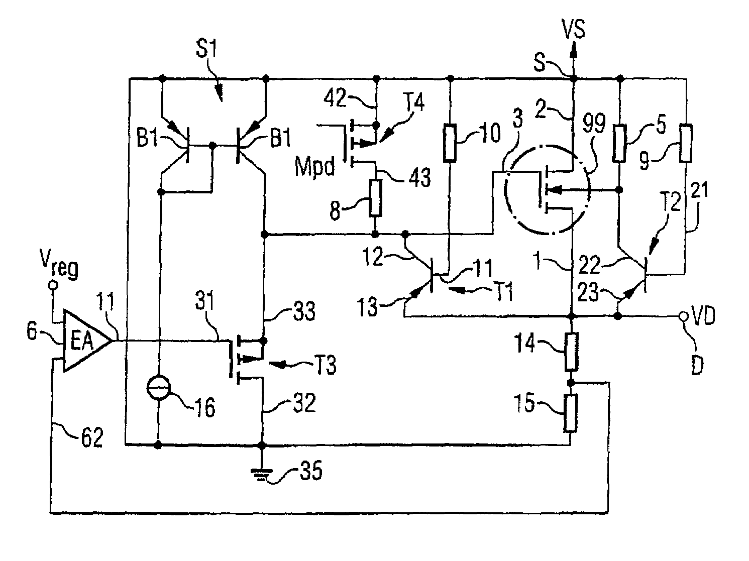
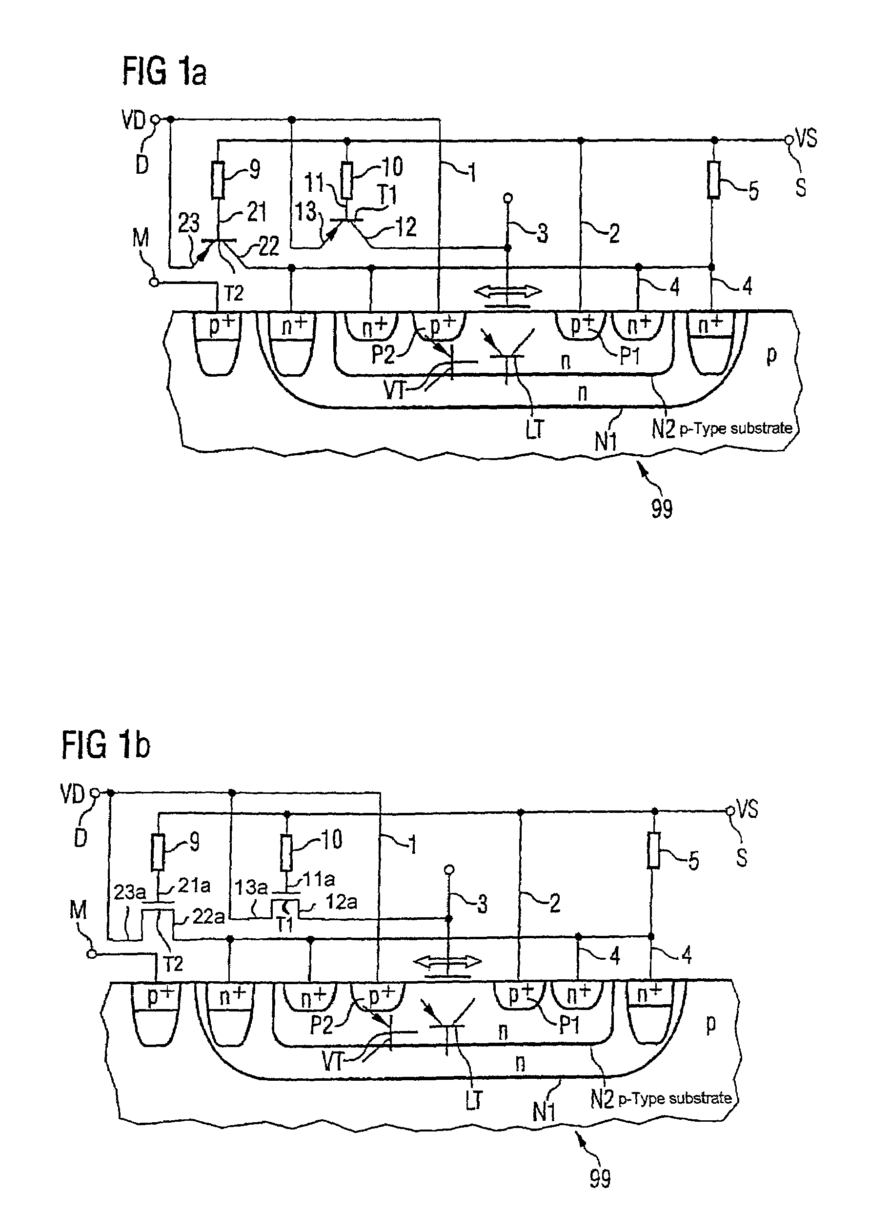
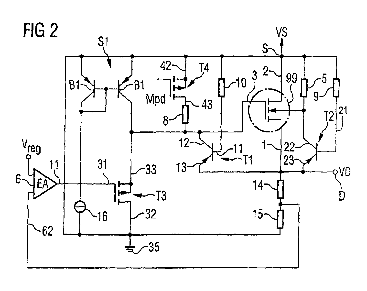
[0027]FIG. 1a shows a circuit arrangement having a PMOS field-effect transistor in which an undesirable current flow is prevented.

[0028]The PMOS transistor 99 is formed in a doped semiconductor substrate. The semiconductor substrate is p-doped and contains a heavily p-doped region p+ for a connection to ground. Within the substrate, an n-doped region is formed as a well which, for its part, is subdivided into two n-doped partial regions N1 and N2 having different doping concentrations. The region N2 is an n-doped partial well in which two heavily p-doped regions P1 and P2 are embedded. The region P1 is called the source of the PMOS transistor 99 and furthermore has a source terminal 2. The region P2 represents the drain and contains the drain terminal 1. Between the source region P1 and drain region P2, a charge carrier channel can form through application of a potential to the control input 3 and the control electrode (not shown here) or a channel that has formed can be altered. P-...


PUM


Abstract

A circuit arrangement for protection against electrostatic discharge for a field-effect transistor is disclosed. The arrangement includes a first and a second controllable path each having a control terminal. The control terminals of the controllable paths are coupled to a source terminal of the field-effect transistor. A first terminal of the first controllable path is connected to a control terminal of the transistor, and a first terminal of the second controllable path is connected to a bulk terminal of the unipolar transistor. Second terminals of the controllable paths are connected to the drain terminal. A voltage regulating device includes the circuit arrangement and a comparator configured to generate a control signal in a manner dependent on a difference between two signals applied thereto. A control output of the comparator is coupled to the control terminal of the transistor.

Description

REFERENCE TO RELATED APPLICATION[0001]This application claims the benefit of the priority date of German application DE 103 40 603.4, filed on Sep. 1, 2003, the contents of which are herein incorporated by reference in their entirety.FIELD OF THE INVENTION[0002]The invention relates to a circuit arrangement. The invention furthermore relates to a voltage regulating device having a circuit arrangement.BACKGROUND OF THE INVENTION[0003]Battery-operated apparatuses such as mobile telephones, laptops or PDAs often require different supply voltages for their individual circuits. For this purpose, they use voltage regulators that transform the voltage supplied by the battery into the required supply voltage. The output voltage of such a voltage regulator is often close to the battery voltage. For such cases, voltage regulators are usually realized with MOS transistors as output stages, because these have the advantage over bipolar transistors that they can also realize small voltage differ...

Claims


Application Information

Patent Timeline
Patent Type & Authority Patents(United States)
IPC IPC(8): H02H3/00H01L23/58H01L23/60H01L27/02H01L29/76H02H9/00H03K17/082
CPCH01L27/0251H03K17/0822
Inventor MULLAUER, MARKUSRIEDERER, ROMAN
Owner INFINEON TECH AG
Why Eureka
Try Eureka