Multi-channel transistor structure and method of making thereof

a transistor and multi-channel technology, applied in transistors, solid-state devices, nanoinformatics, etc., can solve problems such as difficult scaling of existing bulk mosfet devices

Inactive Publication Date: 2008-04-08
TAIWAN SEMICON MFG CO LTD
View PDF21 Cites 40 Cited by
  • Summary
  • Abstract
  • Description
  • Claims
  • Application Information

AI Technical Summary

Problems solved by technology

Due to limitations associated with existing gate-oxide thicknesses and source / drain (S / D) junction depths, scaling of existing bulk MOSFET devices has proven difficult and therefore, alternate device structures, are likely to be needed to improve FET performance.

Method used


Image

  • Multi-channel transistor structure and method of making thereof
  • Multi-channel transistor structure and method of making thereof
  • Multi-channel transistor structure and method of making thereof

Examples


Embodiment Construction

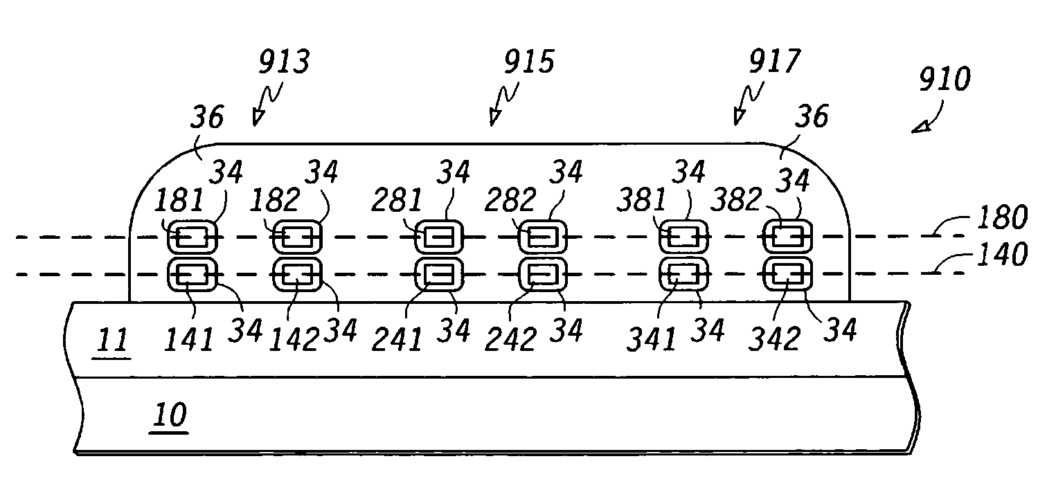
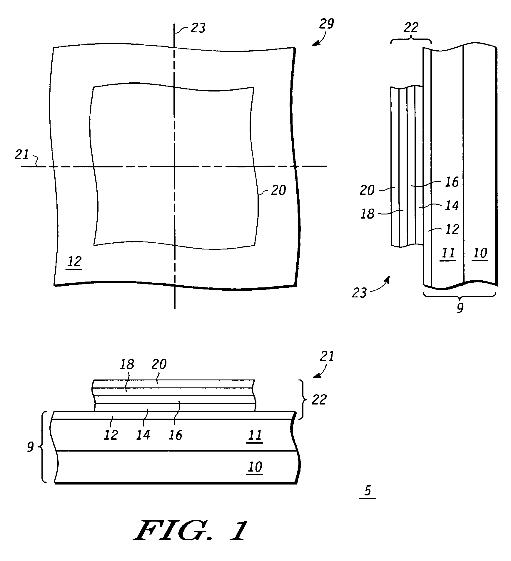
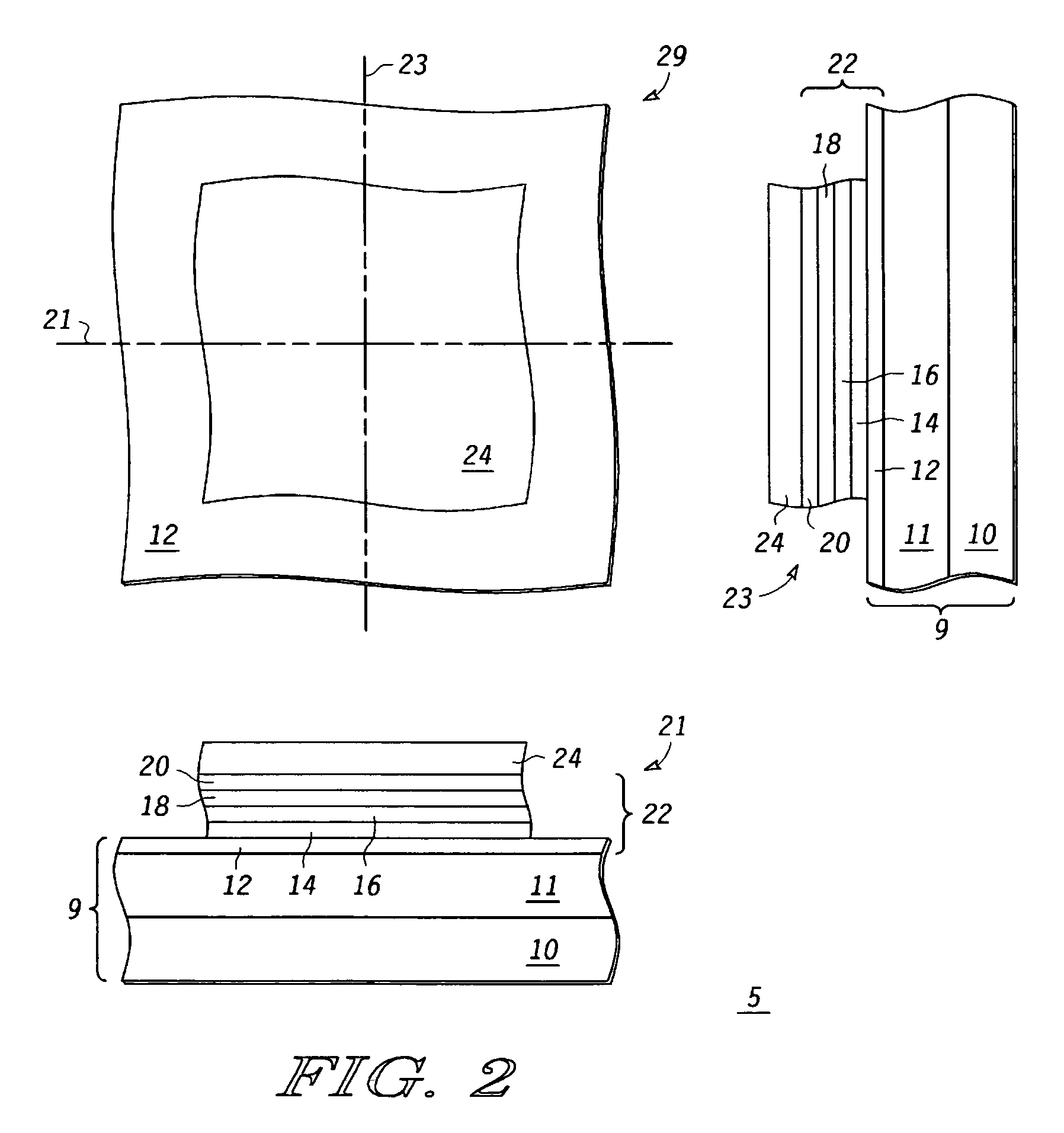
[0032]A semiconductor device having a FinFET-type transistor is disclosed. In a specific embodiment multiple pairs of channels connect a transistor's source / drain regions. The method disclosed facilitates formation of quantum wire channel regions at small dimensions using currently available processes and resulting in transistor performance expected to be characterized by quantized electronic transport in the channel cross-section and ballistic transport in the source-drain current direction. The use of a gate surrounding the channels results in greatly improved short-channel behavior of the device. The scaling potential of the disclosed methods is substantial, with deployment likely with 65 nm and smaller technologies. Another benefit is that formation of a superior transistor as disclosed can further delay the development and deployment of unproven high-k dielectrics. Specific aspects of the present disclosure will be better understood with reference to FIGS. 1-19.

[0033]Before add...


PUM


Abstract

A method of forming an electronic device includes, forming a first channel coupled to a first current electrode and a second current electrode and forming a second channel coupled to the first current electrode and the second current electrode. The method also includes the second channel being substantially parallel to the first channel within a first plane, wherein the first plane is parallel to a major surface of a substrate over which the first channel lies. A gate electrode is formed surrounding the first channel and the second channel in a second plane, wherein the second plane is perpendicular to the major surface of the substrate. The resulting semiconductor device has a plurality of locations with a plurality of channels at each location. At small dimensions the channels form quantum wires connecting the source and drain.

Description

CROSS-REFERENCE TO RELATED APPLICATION(S)[0001]The present application is related to: U.S. Pat. No. 6,921,700 entitled “METHOD OF FORMING A TRANSISTOR HAVING MULTIPLE CHANNELS”, filed on Jul. 31, 2003 which is hereby incorporated by reference herein in its entirety.BACKGROUND[0002]1. Field of the Disclosure[0003]This disclosure relates generally to electronic devices, and particularly to manufacturing electronic devices having transistors with one or more channels.[0004]2. Description of the Related Art[0005]Scaling of device dimensions has been a primary factor driving improvements in integrated circuit performance and reduction in integrated circuit cost. Due to limitations associated with existing gate-oxide thicknesses and source / drain (S / D) junction depths, scaling of existing bulk MOSFET devices has proven difficult and therefore, alternate device structures, are likely to be needed to improve FET performance.[0006]Transistors with alternative channel designs are particularly ...

Claims


Application Information

Patent Timeline
Patent Type & Authority Patents(United States)
IPC IPC(8): H01L21/336H01L21/00H01L21/84H01L27/01H01L27/12H01L31/0392
CPCB82Y10/00H01L29/0673H01L29/1029H01L29/42392H01L29/775H01L29/78696H01L2924/0002H01L2924/00
Inventor ORLOWSKI, MARIUS K.
Owner TAIWAN SEMICON MFG CO LTD
Why Eureka
Try Eureka