Hermetic MEMS package and method of manufacture

a technology of mems and packaging, applied in the direction of microstructured systems, semiconductor devices, semiconductor/solid-state device details, etc., can solve the problems of affecting the performance of unpassivated devices, unable to eliminate device heating altogether, and a large amount of heat transmitted through the package base and into the active device, etc., to achieve a high degree of hermeticity

Inactive Publication Date: 2008-04-15
STELLAR MICRO DEVICES
View PDF7 Cites 39 Cited by
  • Summary
  • Abstract
  • Description
  • Claims
  • Application Information

AI Technical Summary

Benefits of technology

[0021]A further object and advantage of the invention is to form such gasket, cutting and flowing edge and locking mechanism on a substrate at the wafer scale thus enabling the basic bonding technology to be extended to wafer scale hermetic packaging.
[0022]Another object and advantage of the invention is to form a hermetic seal at room temperature with such seal exhibiting a leak rate of less than 10^-9 Torr liter / sec.
[0023]A specific advantage of the invention is a method of room temperature hermetic sealing of MEMS devices that exhibit sensitivity to heat cycling during the sealing operation.
[0024]Another advantage of the invention is very high thruput sealing since only a single compression step is required for making a hermetic seal. No heat cycling with attendant solder melt or welding dwell times is required.
[0025]Another advantage of the invention is its application to microdevices other than MEMS such as hybrid assemblies and semiconductor devices for example where they may require a high degree of hermeticity.BRIEF SUMMARY OF THE INVENTION
[0026]An invention is disclosed which utilizes a copper gasket and cutting edge swaging technology to form a hermetic MEMS or microdevice package. In the single die packaging embodiment conventional semiconductor packages are modified or new packages are developed to provide a cutting edge structure on one or both of the cap and base. An integral, plated or separate metal gasket is provided to implement the hermetic seal. A metal forming structure is provided for maintaining force on the cap and base assembly after hermetic compression. The metal forming structure is actuated simultaneously with compression bonding through the use of a compound bonding head die.

Problems solved by technology

Both of these techniques result in a considerable amount of heat transmitted through the package base and into the active device.
Although there are methods of reducing the amount of heat transfer to the active device it is not possible to eliminate the device heating altogether.
In addition to the active device heating described above heat generated at the sealing surfaces releases contaminants to the inside of the package which can affect the performance of unpassivated devices.
This can be especially destructive to unpassivated MEMS devices where micro mechanical moving parts are fully exposed to released contaminants due to the sealing heat cycle.
However due to residual stress in free standing members and the extreme sensitivity of structure surfaces to contamination more complex MEMS devices cannot tolerate heat during the packaging operation.
However once release is performed the MEMS devices cannot be singulated without the individual mechanical parts being damaged or becoming stuck together (called stiction).

Method used


Image

  • Hermetic MEMS package and method of manufacture
  • Hermetic MEMS package and method of manufacture
  • Hermetic MEMS package and method of manufacture

Examples


Embodiment Construction

[0036]Although the following detailed description delineates many specific attributes of the invention and describes specific fabrication procedures those skilled in the art of microfabrication will realize that many variations and alterations in the fabrication details and the basic structures are possible without departing from the generality of the processes and structures. The most general attributes of the invention relate to a structure and method of making a hermetic seal between a package base and cap at room temperature.

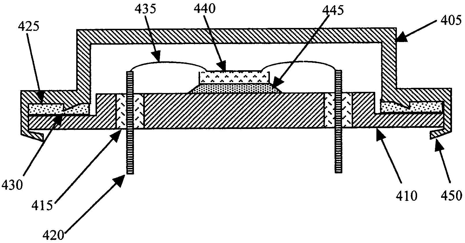
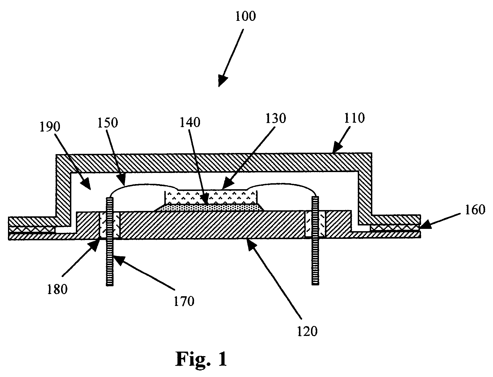
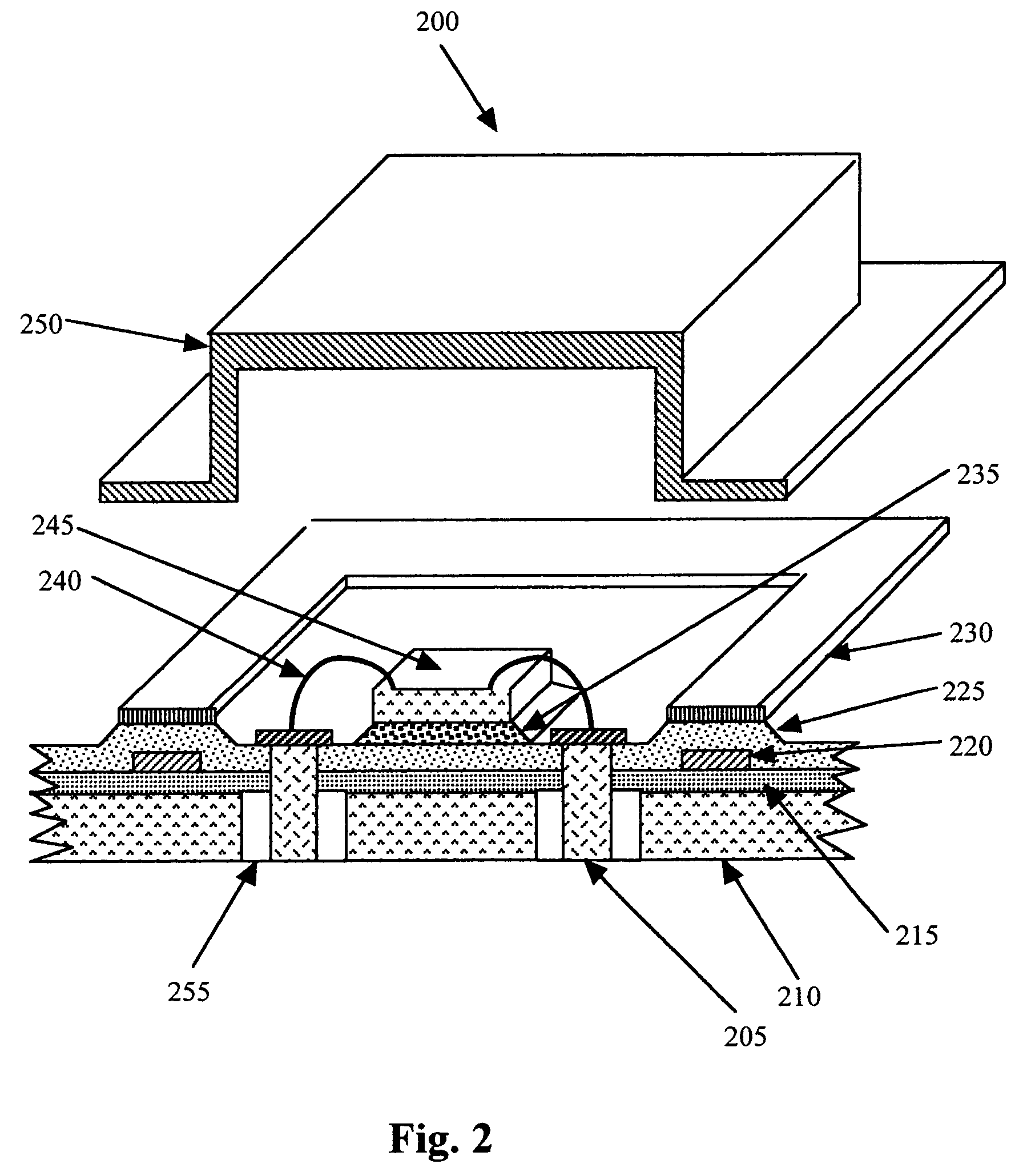
[0037]Extensive prior art in the packaging of microdevices is shown in FIGS. 1, 2 and 3. FIG. 1 delineates a hypothetical MEMS device 130 mounted on package base 120 with electrical feedthrus 170 penetrating the base and insulated from the base by insulator 180. MEMS device 130 is attached to the base 120 using material 140 which may typically be solder or organic adhesive. Wire bonds 150 connect the MEMS device electrically to feedthrus 170. MEMS die 130 ma...


PUM


Abstract

A swage hermetic sealing of a MEMS or microdevice or nanodevice package using high force. A cutting and flowing edge 430 is formed on a package cover which is pressed into a mating , integral gasket 425 on a package base. A material extension of the package cover 450 is simultaneously folded under the package base to supply force maintenance for permanent hermaticity. The swage hermetic sealing of single or an array of covers to an extended wafer or substrate is accomplished by a cutting and flowing edge 560. Permanent force maintenance is achieved through a re-entrant cavity 565 and annular ring 535 on the wafer or substrate.

Description

CROSS REFERENCE TO RELATED APPLICATION[0001]This application claims benefit of U.S. Provisional Patent application Ser. No. 60 / 550,844 filed Mar. 8, 2004 and Disclosure Document No. 542148, filed Nov. 17, 2003. Subject matter set forth in Provisional Patent No. 60 / 550,844 and Disclosure Document No. 542148 is hereby incorporated by reference into the present application as if fully set forth herein.STATEMENT REGARDING FEDERALLY FUNDED REASERCH AND DEVELOPMENT[0002]NoneBACKGROUND OF THE INVENTION[0003]Hermetic microdevice packages enjoy wide use in the semiconductor industry in applications where true hermeticity is required. Such hermeticity is required where any outside of the package ambient conditions or variations in the ambient conditions might affect device performance. Generally in the semiconductor industry hermetic passivation layers have been developed and applied to the surface of sensitive devices in order to give a primary level of defense against ambient conditions. So...

Claims


Application Information

Patent Timeline
Patent Type & Authority Patents(United States)
IPC IPC(8): H01L21/00
CPCB81C1/00269B81C2203/0109H01L21/50H01L23/045H01L23/10H01L2224/48137H01L2224/4823H01L2224/73265H01L2924/01046H01L2924/01078H01L2924/01079H01L2924/09701H01L2924/16152H01L2924/16315H01L2924/01322
Inventor POTTER, CURTIS NATHAN
Owner STELLAR MICRO DEVICES
Why Eureka
Try Eureka