

Method for driving plasma display panel
- Summary
- Abstract
- Description
- Claims
- Application Information
AI Technical Summary
Benefits of technology
Problems solved by technology
Method used
Image

Examples
first embodiment
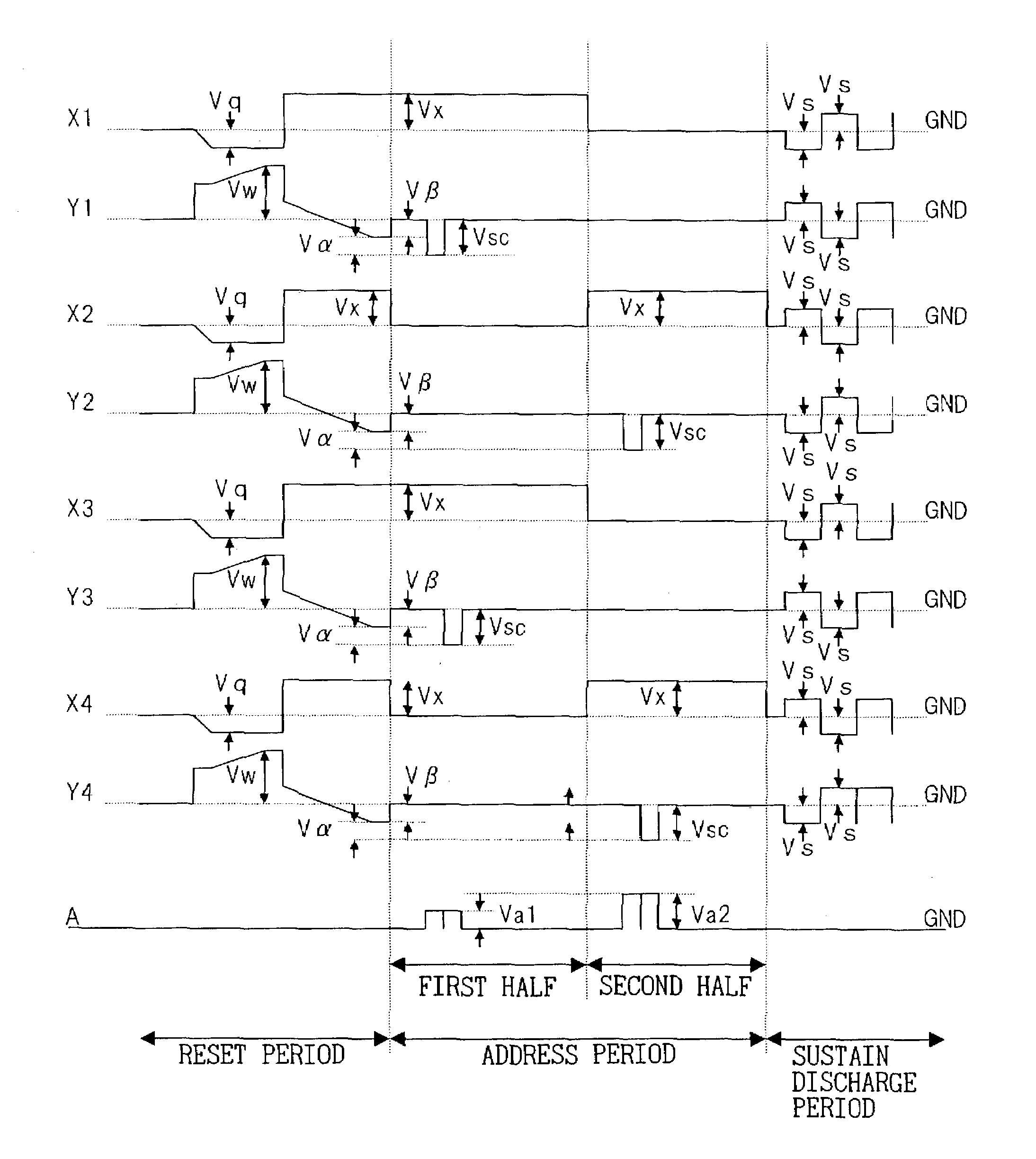
[0054]FIG. 10 shows the waveforms that illustrate the method for driving an AC-driven PDP in the present invention.
[0055]FIG. 10 shows a driving method in a subfield, and waveforms in the address (A) electrodes, the sustain electrodes X1 to X4 and the scan electrodes Y1 to Y4 in an arbitrary subfield in a field where the display in the odd-numbered lines and even-numbered lines is performed.
[0056]First, as shown in FIG. 10, in the reset action in the first half of the reset period, while all the address electrodes are kept at 0 (V) by the address driver 12, a negative pulse and a positive pulse are applied to every sustain electrode X and scan electrode Y, respectively. In other words, a pulse having a voltage −Vq is supplied to every sustain electrode X from the odd-numbered X sustain circuit 13a and the even-numbered X sustain circuit 13b, and at the same time a pulse having a voltage Vw is applied to every scan electrode Y from the odd-numbered Y sustain circuit 14a and the even-...
second embodiment
[0074]Next, the present invention is described below.
[0075]FIG. 11 is a diagram that shows the method for driving an AC-driven PDP in the second embodiment of the present invention. In the following description, the same symbols are assigned to the components that are the same as those described above, and only the difference is described, with just reference to those components.
[0076]As is obvious from the comparison between FIG. 11 an FIG. 10, the driving method in the present embodiment differs from that in the first embodiment in that the voltage applied to each X electrode and Y electrode in the odd-numbered lines and even-numbered lines in the reset period (first half and second half) and address period is identical (value), and the voltage Va2 applied to the address electrode during the scanning of the even-numbered lines in the second half of the address period is set to a value larger than the voltage Va1 applied to the address electrode during the scanning of the odd-numbe...
PUM
 Abstract
Description
Claims
Application Information