Three dimensional integrated circuit and method of making the same

a three-dimensional integrated circuit and integrated circuit technology, applied in the field of three-dimensional (3d) integrated circuits, can solve the problems of affecting the budget of integrated circuits, affecting the performance of integrated circuits, and consuming more power in the interconnect structur

Active Publication Date: 2008-06-10
TAIWAN SEMICON MFG CO LTD
View PDF26 Cites 195 Cited by
  • Summary
  • Abstract
  • Description
  • Claims
  • Application Information

AI Technical Summary

Problems solved by technology

As feature sizes of integrated circuits continue to shrink to meet performance demands and overall chip dimensions increase, the interconnect structure consumes more of the available power and delay budgets for integrated circuits.
For advanced devices with low dielectric constant (low k) materials, this process may induce failure of the low k materials.
Adhesive bonding typically employs BCB (BenzoCycloButene), which has a glass transition temperature of 350° C. The bonding material is unstable during subsequent higher temperature processes utilized in completing the device interconnections.

Method used


Image

  • Three dimensional integrated circuit and method of making the same
  • Three dimensional integrated circuit and method of making the same
  • Three dimensional integrated circuit and method of making the same

Examples


Embodiment Construction

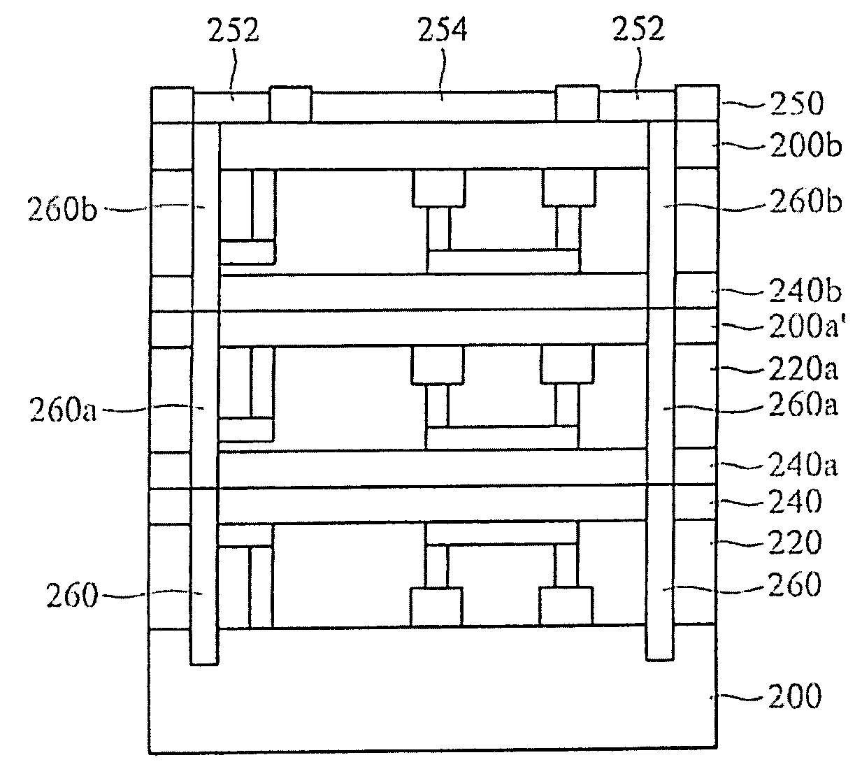
[0013]As sometimes used herein, three-dimensional integration refers to any process by which multiple conventional device layers may be stacked and electrically interconnected. Three dimensional integration provides benefits in terms of wire length, area, timing and energy consumption.

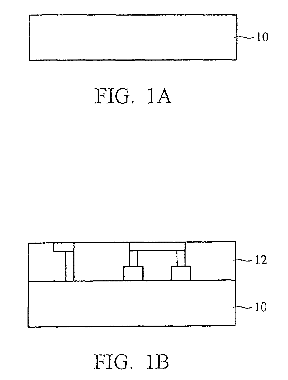
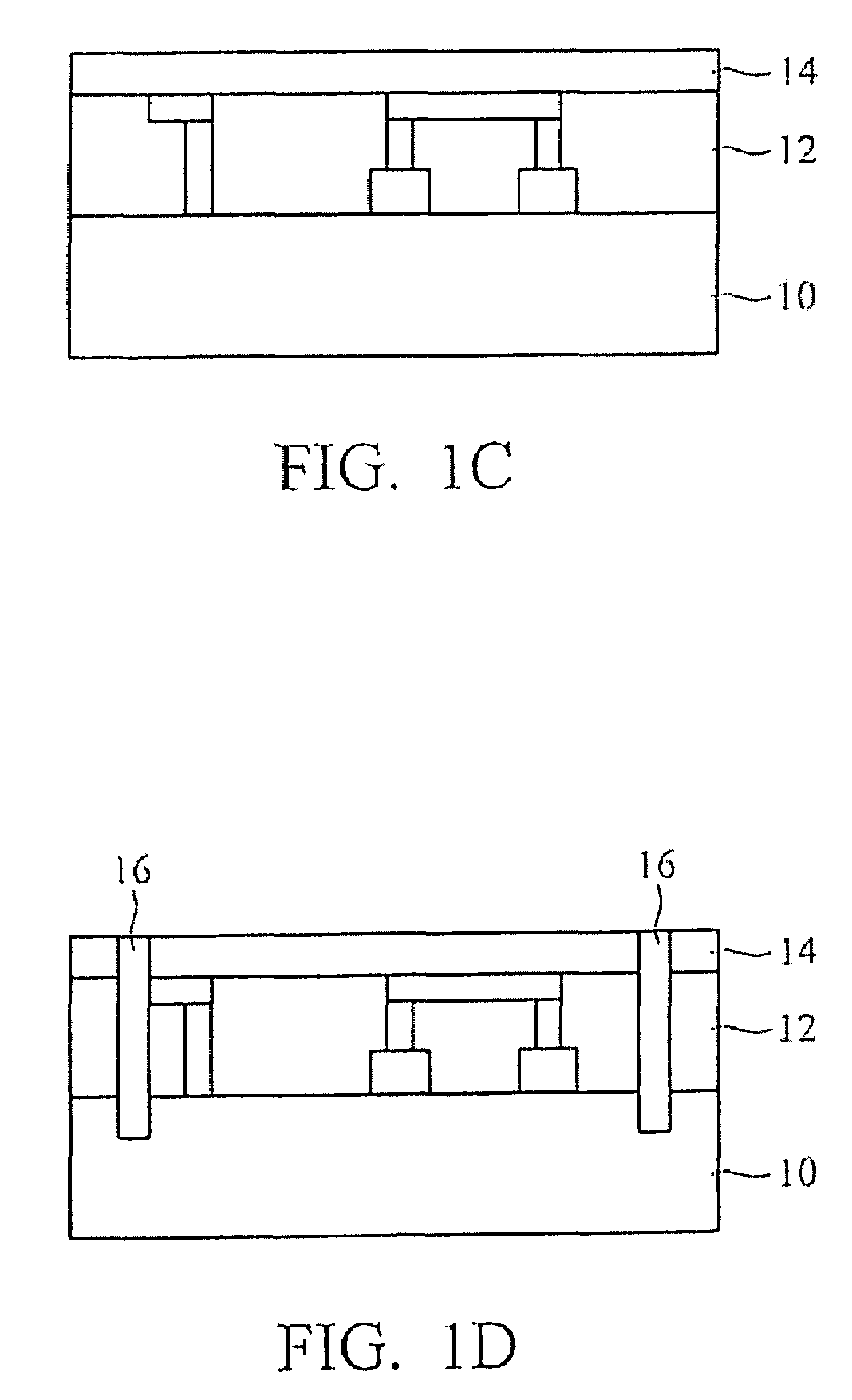
[0014]FIGS. 1-3 illustrate various embodiments of methods of forming three-dimensional integrated circuits and three-dimensional integrated circuits formed thereby.

[0015]As shown in FIG. 1A, a substrate 10 is provided. Substrate 10 preferably comprises a silicon substrate although other semiconductor substrates, such as silicon-germanium substrate, III-V compound substrate, or silicon on insulator (SOI) substrate may be utilized in embodiments. At FIG. 1B, the silicon substrate 10 is processed to form a device layer 12. As those in the art will understand, the device layer 12 includes one or more transistors, such as MOS transistors, capacitors or other devices formed over and / or in an active region. F...


PUM


Abstract

A three dimensional integrated circuit structure includes at least first and second devices, each device comprising a substrate and a device layer formed over the substrate, the first and second devices being bonded together in a stack, wherein the bond between the first and second devices comprises a metal-to-metal bond and a non-metal-to-non-metal bond.

Description

FIELD OF THE INVENTION[0001]The present invention relates generally to integrated circuits, and more specifically to three dimensional (3D) integrated circuits. The invention also relates to interconnect and bonding structures and methods of forming interconnects and bonding structures.BACKGROUND OF THE INVENTION[0002]As feature sizes of integrated circuits continue to shrink to meet performance demands and overall chip dimensions increase, the interconnect structure consumes more of the available power and delay budgets for integrated circuits. As wiring has become more expensive and clock frequencies have increased, designers have investigated three-dimensional integration as a means of reducing signaling across chips.[0003]Three dimensional integrated circuits have multiple layers of active components. The active components can be wired to devices on the same and / or different layers. In one approach, multiple conventional wafers are arranged together in a stack with some means of...

Claims


Application Information

Patent Timeline
Patent Type & Authority Patents(United States)
IPC IPC(8): H01L23/02H01L21/00
CPCH01L21/6835H01L23/481H01L24/83H01L25/0657H01L25/50H01L2924/13091H01L2221/6835H01L2221/68363H01L2221/68372H01L2221/68377H01L2224/81894H01L2224/83894H01L2225/06513H01L2225/06517H01L2225/06541H01L2924/01013H01L2924/01029H01L2924/01032H01L2924/14H01L2924/1433H01L2924/19041H01L2924/01006H01L2924/01019H01L2924/01023H01L2924/01033H01L2924/01074H01L2924/00H01L2924/15747H01L24/94H01L2224/0401H01L2224/04042H01L2224/94H01L27/0688H01L21/8221H01L2224/83
Inventor WU, WENG-JINCHIOU, WEN-CHIH
Owner TAIWAN SEMICON MFG CO LTD
Why Eureka
Try Eureka