High dynamic range imager with a rolling shutter

a high dynamic range and imager technology, applied in the field of semiconductor imagers, can solve the problems of underexposure and the danger of overexposur

Active Publication Date: 2008-07-08
MICRON TECH INC
View PDF4 Cites 51 Cited by
  • Summary
  • Abstract
  • Description
  • Claims
  • Application Information

AI Technical Summary

Problems solved by technology

However, for any given integration period, in the presence of incident light having a high level of brightness, there is a danger of overexposure due to the light sensitive element 101 producing too many photo generated charges.
Conversely, in the presence of incident light having a low level of brightness, there is a danger of underexposure due to the light sensitive element 101 producing too few photo generated charges.

Method used


Image

  • High dynamic range imager with a rolling shutter
  • High dynamic range imager with a rolling shutter
  • High dynamic range imager with a rolling shutter

Examples


Embodiment Construction

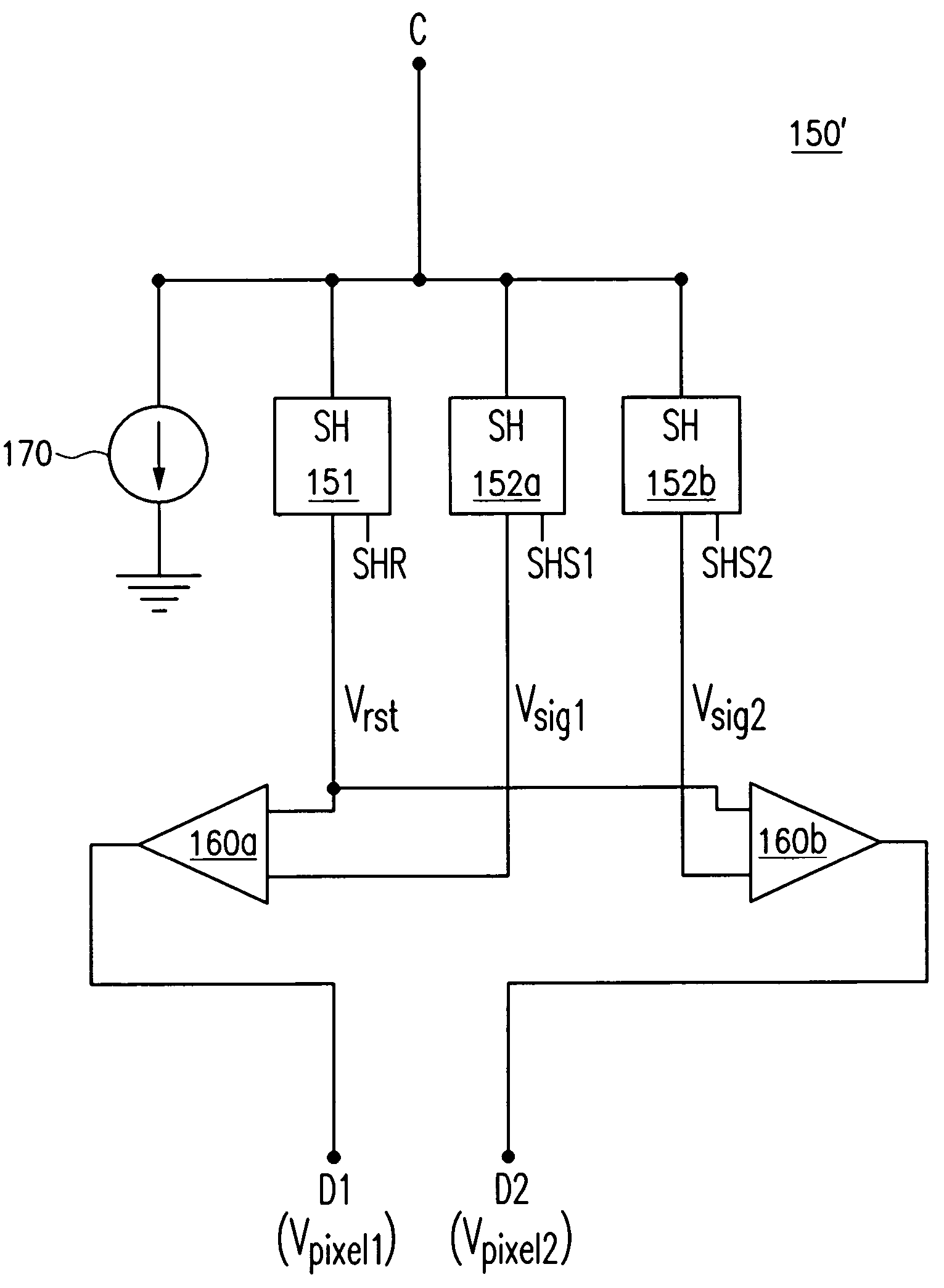
[0020]Now referring to the drawings, where like reference numerals designate like elements, there is shown in FIG. 3 a pixel reading circuit 150′ in accordance with an exemplary embodiment of the present invention. The pixel reading circuit 150′ is a replacement for the conventional pixel reading circuit 150 (FIG. 1) and is compatible with the conventional pixel 100. Preferably, the conventional pixel 100 utilizes a pinned photodiode as a light sensitive element 101. The pixel reading circuit 150′ includes one input node C and two output nodes D1, D2. Coupled in parallel to the input node C is a bias circuit 170, a sample and hold circuit 151 for the reset signal Vrst, a short integration (SI) sample and hold circuit 152a for a SI photo signal Vsig1, and a long integration (LI) sample and hold circuit 152b for a LI photo signal Vsig2. In the context of this invention, a short integration time is shorter in duration than a long integration time. The three sample and hold circuits 151...


PUM


Abstract

A high dynamic range imager operates pixels utilizing at least a short integration period and a long integration period. The pixel reading circuits of the imager are adapted to process pixel signals corresponding to the integration periods in parallel. The pixel signals are converted into digital values in parallel. The digital values are each linear functions of the incident light and therefore suitable for use with conventional color processing algorithms. A pipelined rolling shutter operation may be employed where the short integration period of one row of pixels is performed simultaneously with the long integration period of another row of pixels.

Description

FIELD OF INVENTION[0001]The present invention relates generally to semiconductor imagers. More specifically, the present invention relates to methods and apparatus for a semiconductor imager capable of imaging over a high dynamic range of brightness levels.BACKGROUND OF THE INVENTION[0002]FIG. 1 illustrates a conventional four transistor (4T) imager pixel 100 coupled via column line 125 to a conventional pixel reading circuit 150. The pixel 100 includes a light sensitive element 101, reset, source follower, row select, and transfer transistors 110-114, and nodes A, B, E, and P. Control signals RESET, TX, and ROW are respectively applied to the gates of the reset transistor 110, the transfer transistor 114, and the row select transistor 112. Node A is connected to a supply voltage source (VAAPIX) for the pixel 100. Node E is a floating diffusion, i.e., a charge storage node. Node P is a charge accumulation node of the light sensitive element 101. The outputs produced by the pixel 100...

Claims


Application Information

Patent Timeline
Patent Type & Authority Patents(United States)
IPC IPC(8): H04N5/335H04N5/353H04N5/355H04N5/363H04N5/378
CPCH04N5/235H04N5/335H04N5/2355H04N23/70H04N23/741H04N25/589H04N25/00
Inventor KRYMSKI, ALEXANDER
Owner MICRON TECH INC
Why Eureka
Try Eureka