Wafer measuring fixture

a technology of measuring fixture and wafer, which is applied in the direction of measuring device, structural/machine measurement, instruments, etc., can solve the problems of difficulty in maintenance, large number of steps to be carried out to form the required integrated circuit, and often found broken wafers, so as to prevent further damage, increase yield, and avoid erroneous determination of defects

Active Publication Date: 2008-10-07
POWERCHIP SEMICON MFG CORP
View PDF5 Cites 3 Cited by
  • Summary
  • Abstract
  • Description
  • Claims
  • Application Information

AI Technical Summary

Benefits of technology

[0007]Accordingly, at least one objective of the present invention is to provide a wafer-measuring fixture that can prevent a broken wafer from secondary damages and rapidly perform a measurement to find the actual reason of defects.
[0020]In the present invention, a wafer-measuring fixture is used instead of a plastic bag to hold a broken wafer. Thus, the broken wafer can be well-maintained and secondary damages to the wafer which may lead to an erroneous determination of the reason of defects can be eliminated. Furthermore, the scale marks around the wafer-measuring fixture can help quickly locate the broken positions in the wafer and find the reason of defects to prevent further damages. In other words, the present invention provides a means of increasing the yield and lowering the production cost by reducing damages.

Problems solved by technology

As a result, a considerable number of steps need to be carried out to form the required integrated circuits on the silicon substrate.
In the process of fabricating the integrated circuit devices, wafers are often found broken.
However, the inappropriate management of the broken wafers conducted by individual operator may result in some issues.
Placing a broken wafer in a general-purpose plastic bag may bring about difficulties of maintenance.
Therefore, the wafer may have secondary damages before any inspection is performed, which may lead to erroneous determination of the reason of defects and to failure of improvement.
Consequently, a lower yield rate and higher production cost of the devices will be incurred.

Method used


Image

  • Wafer measuring fixture
  • Wafer measuring fixture
  • Wafer measuring fixture

Examples


Embodiment Construction

[0028]Reference will now be made in detail to the present preferred embodiments of the invention, examples of which are illustrated in the accompanying drawings. Wherever possible, the same reference numbers are used in the drawings and the description to refer to the same or like parts.

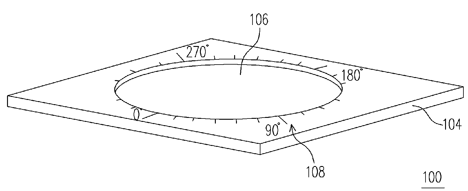
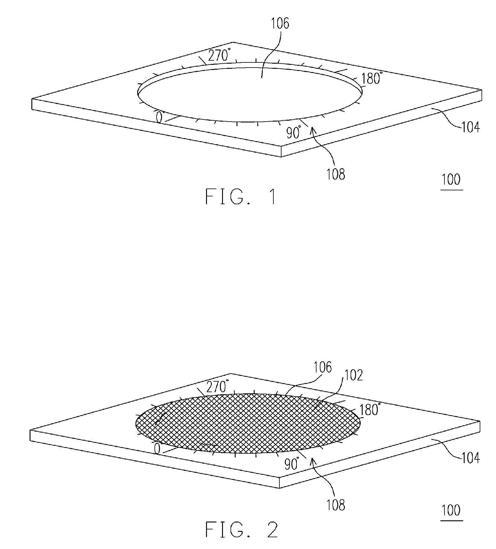
[0029]FIG. 1 is a perspective view of a wafer-measuring fixture according to one embodiment of the present invention. FIG. 2 is a perspective view of the wafer-measuring fixture according to FIG. 1 after inserting a broken wafer.

[0030]As shown in FIGS. 1 and 2, the wafer-measuring fixture 100 provided by the present invention can be used for carrying a broken wafer 102. Here, the broken wafer 102 refers to a wafer having defects such as cracks or splits. The wafer-measuring fixture 100 has a base 104 fabricated using acrylic material, other suitable plastic materials, or even materials such as wood or glass, but most preferably acrylic material.

[0031]The base 104 has a carrying component 106 for hold...


PUM


Abstract

A wafer-measuring fixture suitable for carrying a broken wafer is described. The wafer-measuring fixture comprises a base having a carrying component. The carrying component is used to hold the broken wafer. Furthermore, a plurality of scale marks is set around the carrying component to mark the broken positions on the wafer.

Description

BACKGROUND OF THE INVENTION[0001]1. Field of the Invention[0002]The present invention relates to an apparatus for holding a broken wafer in a factory. More particularly, the present invention relates to a wafer-measuring fixture.[0003]2. Description of the Related Art[0004]As the fabrication of integrated circuit devices advances toward greater density, the dimension of devices defined on a silicon substrate has shrunk so much that the associated circuit design has become very sophisticated. As a result, a considerable number of steps need to be carried out to form the required integrated circuits on the silicon substrate. More specifically, the fabricating process of a particular batch of silicon substrates from raw input to the end of inspection and delivery will be processed among various processing stations.[0005]In the process of fabricating the integrated circuit devices, wafers are often found broken. To prevent the defect from affecting the operation of the processing statio...

Claims


Application Information

Patent Timeline
Patent Type & Authority Patents(United States)
IPC IPC(8): G01M19/00G01M99/00
CPCH01L21/67288H01L21/67353H01L21/67386
Inventor LIN, HUNG-YEN
Owner POWERCHIP SEMICON MFG CORP
Why Eureka
Try Eureka