Plasma display module

a technology of display module and plasma, which is applied in the direction of electrical apparatus casing/cabinet/drawer, earth/grounding circuit, instruments, etc., can solve the problems of increasing manufacturing costs, high raw material cost, and aluminum chassis base being susceptible to bending or twisting, etc., to achieve the effect of adding strength and rigidity

Inactive Publication Date: 2008-10-14
SAMSUNG SDI CO LTD
View PDF4 Cites 21 Cited by
  • Summary
  • Abstract
  • Description
  • Claims
  • Application Information

AI Technical Summary

Benefits of technology

[0016]Preferably the chassis base comprises: a plurality of recesses formed in a rear surface area of the chassis base for receiving the plurality of circuit substrates; and a plurality of coupling bosses for receiving the plurality of screw members, the coupling bosses being formed as an integral part of the chassis base protruding from the recesses. In addition, the chassis base comprises a plurality of ribs framing the plurality of recesses, the ribs providing added strength and rigidity to the chassis base. Further, the non-metallic material forming the chassis base is preferably comprised of a plastic material, a thermoplastic resin material or a thermosetting resin material.
[0018]Additionally, the chassis base comprises: a plurality of recesses formed in a rear surface area of the chassis base for receiving the plurality of circuit substrates; a plurality of coupling bosses for receiving the plurality of screw members, the coupling bosses being formed as an integral part of the chassis base protruding from the recesses, and a plurality of ribs framing the plurality of recesses, the ribs providing added strength and rigidity to the chassis base.
[0019]Further, the plasma display module comprises: flexible connection members having a buffering capability together with electrical conductivity, the flexible connection members being tightly sandwiched between the chassis base and the grounding member, at least one of the flexible connection members forming an electrical connection between the at least one screw member and the grounding member; and a flexible thermal conductive member disposed between the flexible connection members, the flexible thermal conductive member having a buffering capability together with thermal conductivity, the flexible thermal conductive member being tightly sandwiched between the chassis base and the grounding member so that the flexible thermal conductive member can intermediate heat transfer from the chassis base to the grounding member.

Problems solved by technology

Accordingly, the cost of raw materials required may be high, thereby increasing manufacturing costs.
Also, the chassis base formed of an aluminum material may be susceptible to bending or twisting due to its material characteristics.
Therefore, when an external impact is applied to the plasma display module during transportation or moving, the plasma display panel and the circuit substrates cannot be protected by the chassis base, and therefore, may be damaged by the external impact.
In particular, as the size of the plasma display panel increases, the size of the chassis base, which is proportional to the size of the plasma display panel, also increases, and therefore, becomes more susceptible to bending or twisting.
However, the increased thickness is undesirable for making a slim display module.
Overall, the chassis base, formed of an aluminum material, may be a limiting factor in making a lightweight and slim plasma display module.
However, when an insulating plastic material is used for manufacturing the chassis base, the circuit substrates cannot be grounded by conventional grounding method.

Method used


Image

  • Plasma display module
  • Plasma display module
  • Plasma display module

Examples


Embodiment Construction

[0026]The present invention will now be described more fully with reference to the accompanying drawings in which exemplary embodiments of the invention are shown.

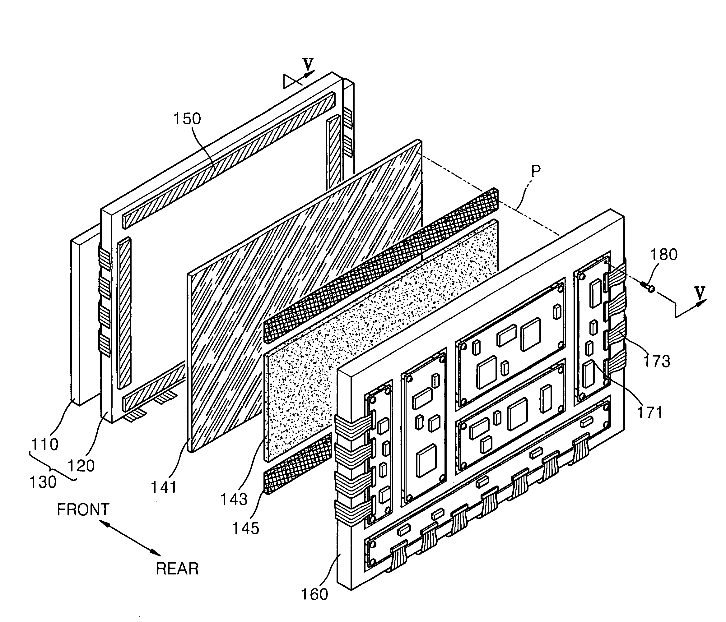
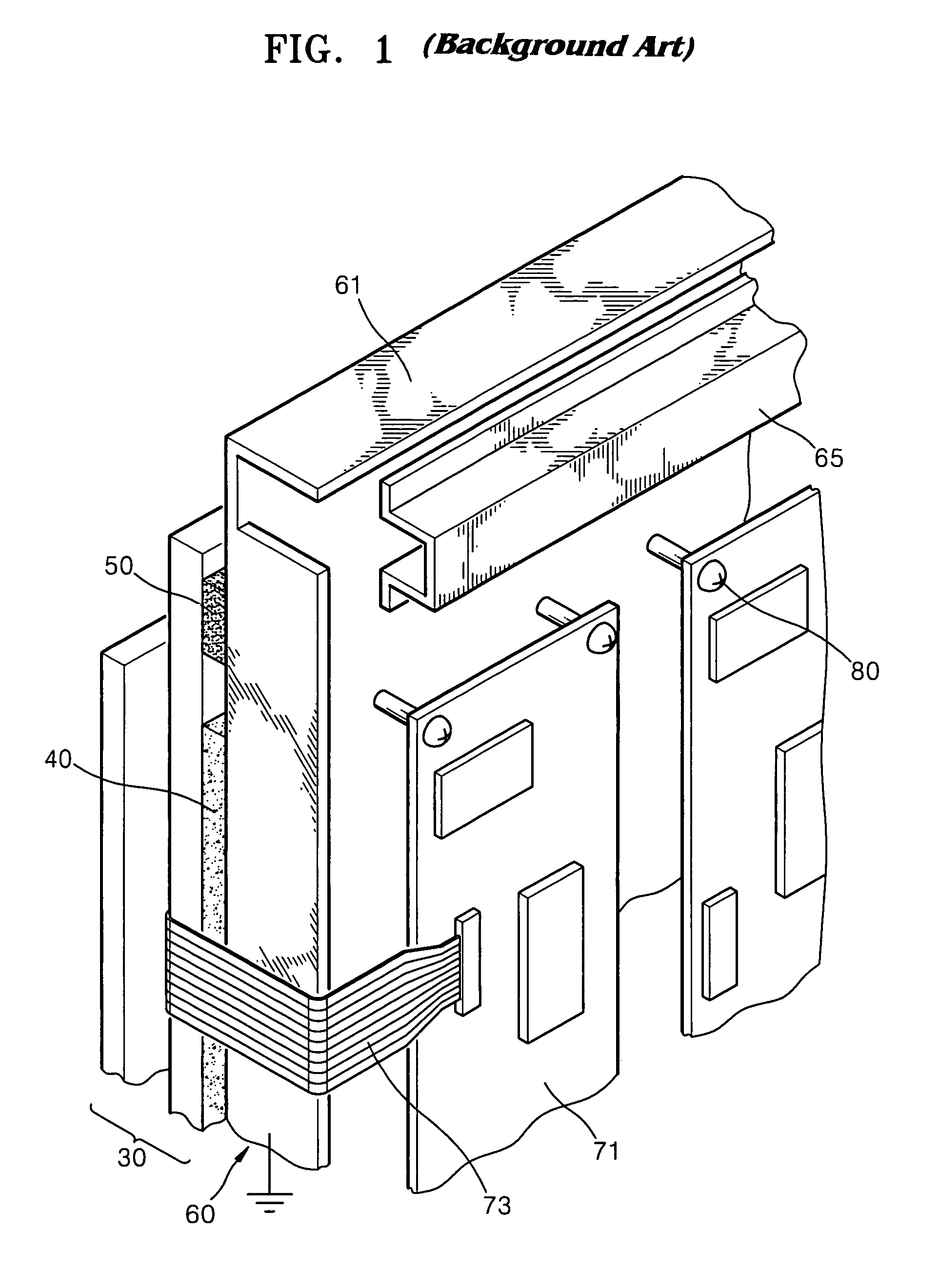
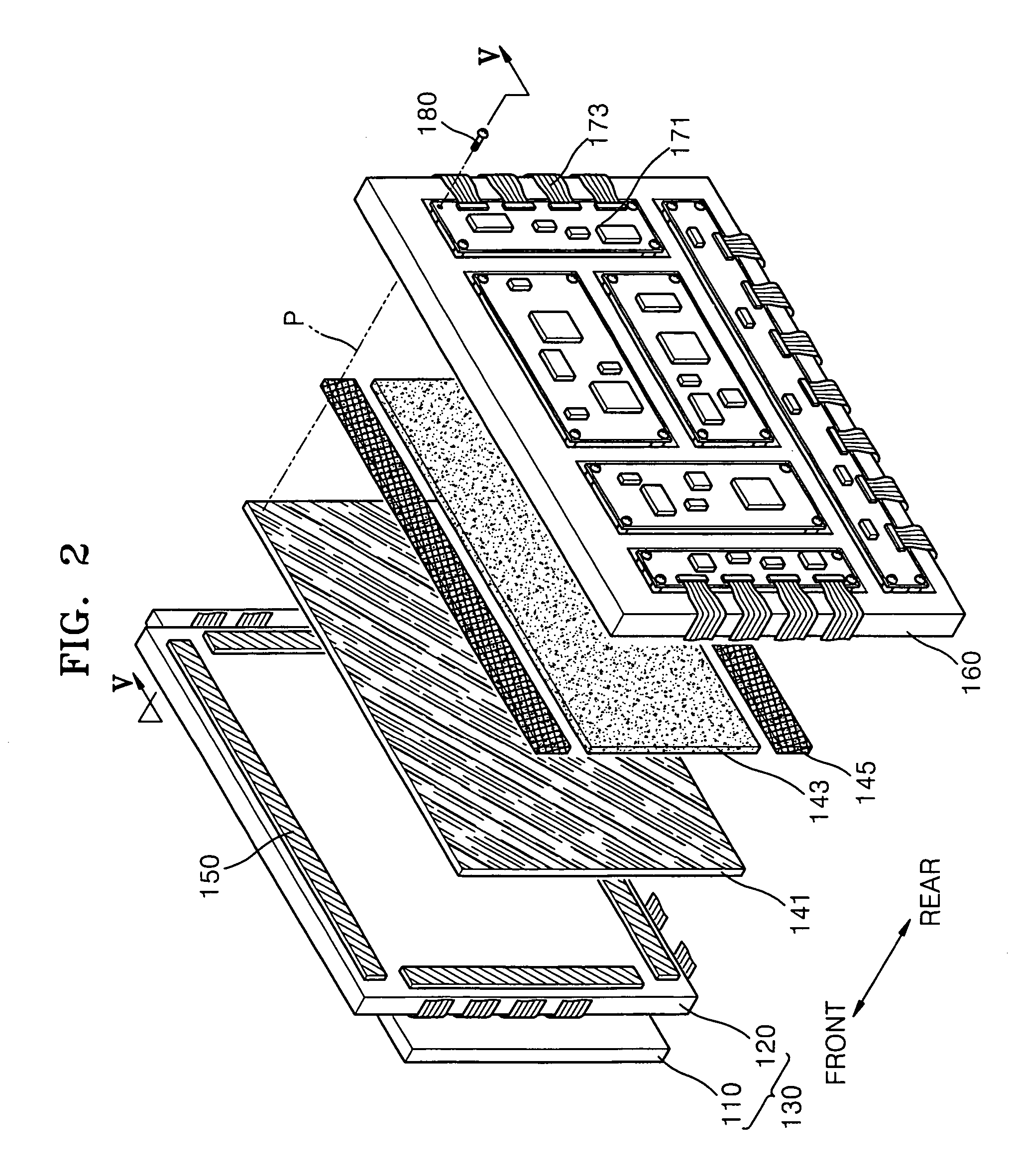
[0027]FIG. 1 is a perspective view of an example of plasma display module. The plasma display module includes a plasma display panel 30 forming a front portion of the plasma display module to display images and a chassis base 60 that supports the plasma display panel 30 from a rear side of the plasma display panel 30. Circuit substrates 71 that generate predetermined driving signals to be applied to the plasma display panel 30 are mounted on a rear surface of the chassis base 60. The driving signals generated by the circuit substrates 71 are transmitted to the plasma display panel 30 through connection cables 73.

[0028]A heat dissipation sheet 40 for transmitting heat generated by the operation of the plasma display panel 30 to the chassis base 60 is interposed between the plasma display panel 30 and the chassis base 60. A ...


PUM


Abstract

A plasma display module having an improved grounding structure suitable for manufacturing a lightweight and slim plasma display module. The plasma display module includes: a chassis base formed of a plastic material; a plasma display panel disposed in front of the chassis base to display images; a plurality of circuit substrates disposed on a rear surface of the chassis base to drive the plasma display panel; a grounding member which is disposed corresponding to the circuit substrates so that the chassis base is disposed between the grounding member and the circuit substrates and is formed of a conductive material so that the grounding member can provide a ground voltage to the circuit substrates grounded to the grounding member; and a screw member that electrically connects the circuit substrates to the grounding member through the chassis base and fixes the circuit substrates to the chassis base.

Description

CLAIM OF PRIORITY[0001]This application makes reference to, incorporates the same herein, and claims all benefits accruing under 35 U.S.C. §119 from an application for PLASMA DISPLAY MODULE earlier filed in the Korean Intellectual Property Office on 6 Dec. 2005 and there duly assigned Serial No. 10-2005-00117843.BACKGROUND OF THE INVENTION[0002]1. Field of the Invention[0003]The present invention relates to a plasma display module, and more particularly, to a plasma display module having an improved circuit substrate grounding structure suitable to be used to manufacture a slim and light weighted display module.[0004]2. Description of the Related Art[0005]Plasma display modules are flat panel display modules that display images by using a discharge effect. Due to their very good characteristics, such as high display capacity, high brightness, high contrast, high performance, clear latent images, wide viewing angles, slim structure, and large screen size, plasma display devices are c...

Claims


Application Information

Patent Timeline
Patent Type & Authority Patents(United States)
IPC IPC(8): G06F1/16H05K5/00H05K7/00
CPCH05K7/20963H01J11/46H01J11/34H05K9/0064H05K3/361
Inventor CHO, IN-SOO
Owner SAMSUNG SDI CO LTD
Why Eureka
Try Eureka