
Optical logic device responsive to pulsed signals

a logic device and pulsed technology, applied in the field of optical logic devices, can solve the problems of difficult to set the delay amount again, the delay amount generated by the delay portion of the electric signal is very difficult, and the delay amount is difficult to determin

Inactive Publication Date: 2008-10-28
YOKOGAWA ELECTRIC CORP
View PDF15 Cites 2 Cited by
  • Summary
  • Abstract
  • Description
  • Claims
  • Application Information

AI Technical Summary

Benefits of technology

[0036]Further, the amplification portion amplifies the electric signal outputted from the photoelectric conversion portion and then outputs the amplified electric signal to the comparator. Thus, logic operations can accurately be performed even when the light intensities of the input light signals are very low.

Problems solved by technology

Furthermore, even among devices of the same kind (for instance, transistors), there are differences in the delay amount.
Thus, the setting of the delay amounts generated by the electric signal delay portion 31 is very difficult.
However, it is very difficult to set again the delay amount.
However, in the case of a high bit rate (for example, 10 Gbps to 40 Gbps), it is very difficult for the electric signal delay portion 31 to perform the delay amount adjustment itself.

Method used


Image

  • Optical logic device responsive to pulsed signals
  • Optical logic device responsive to pulsed signals
  • Optical logic device responsive to pulsed signals

Examples


Embodiment Construction

[0045]Embodiments of the invention are described by referring to the accompanying drawings.

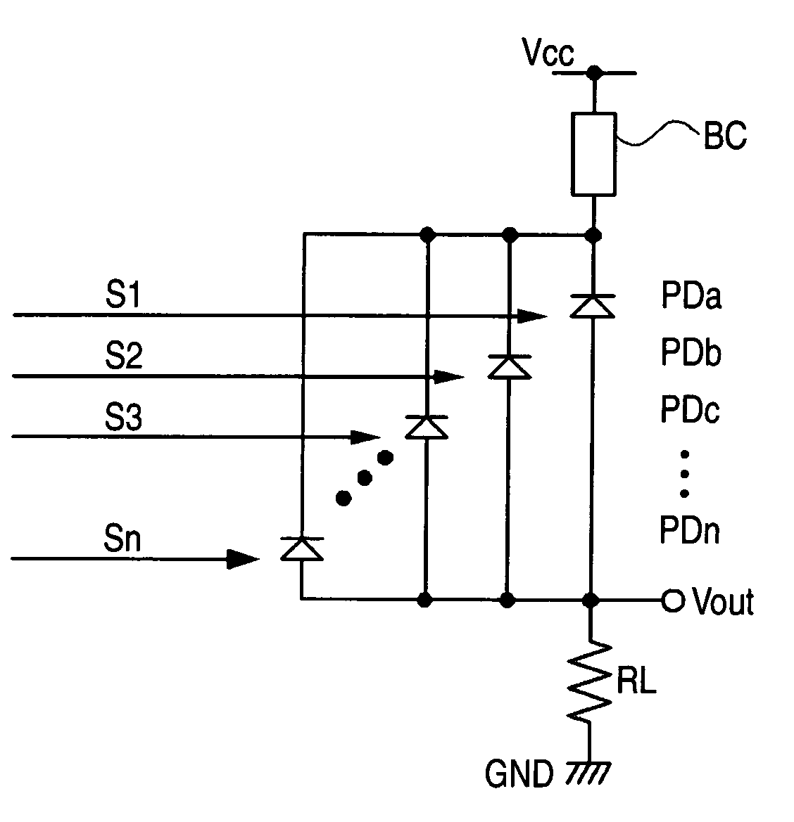
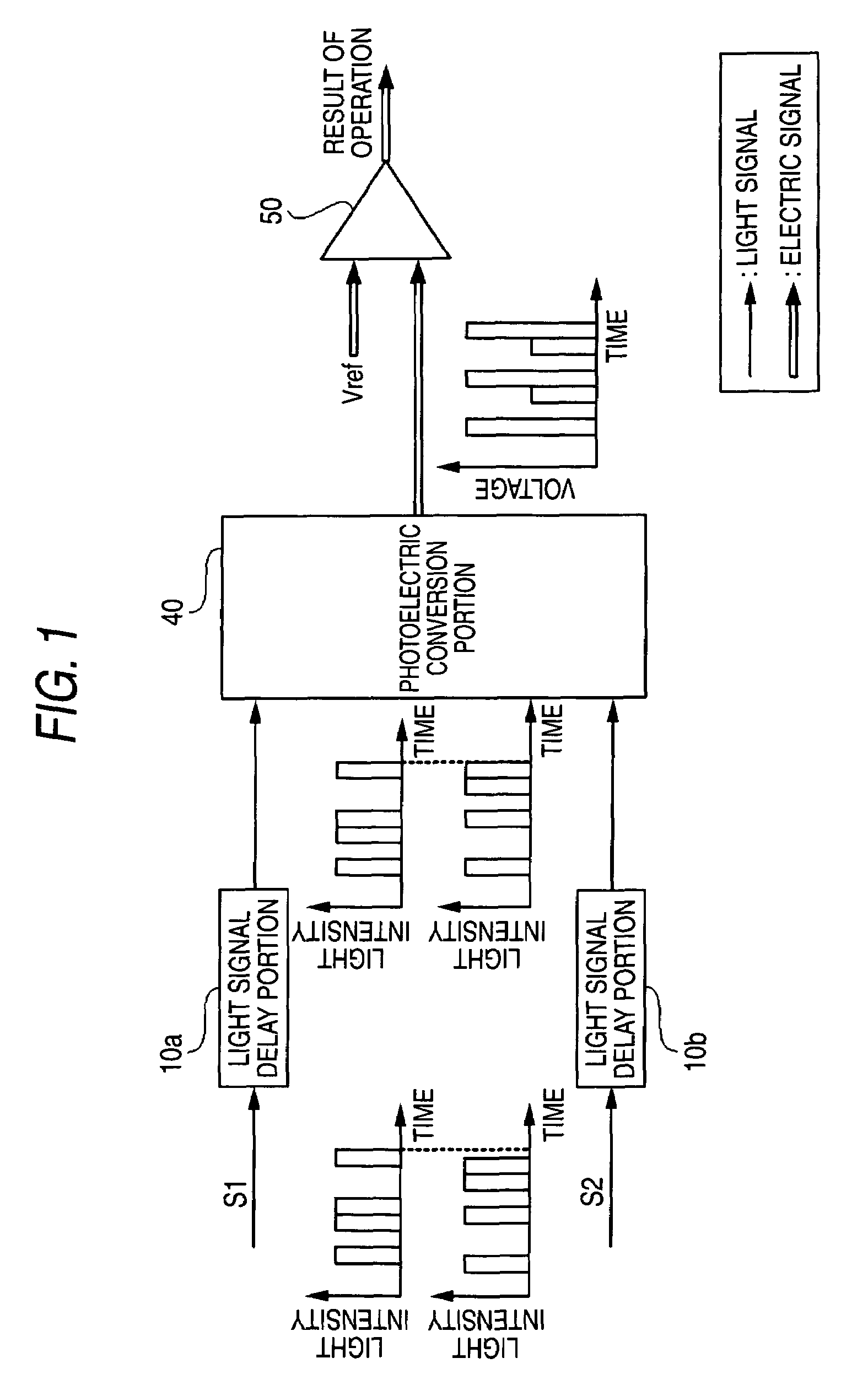
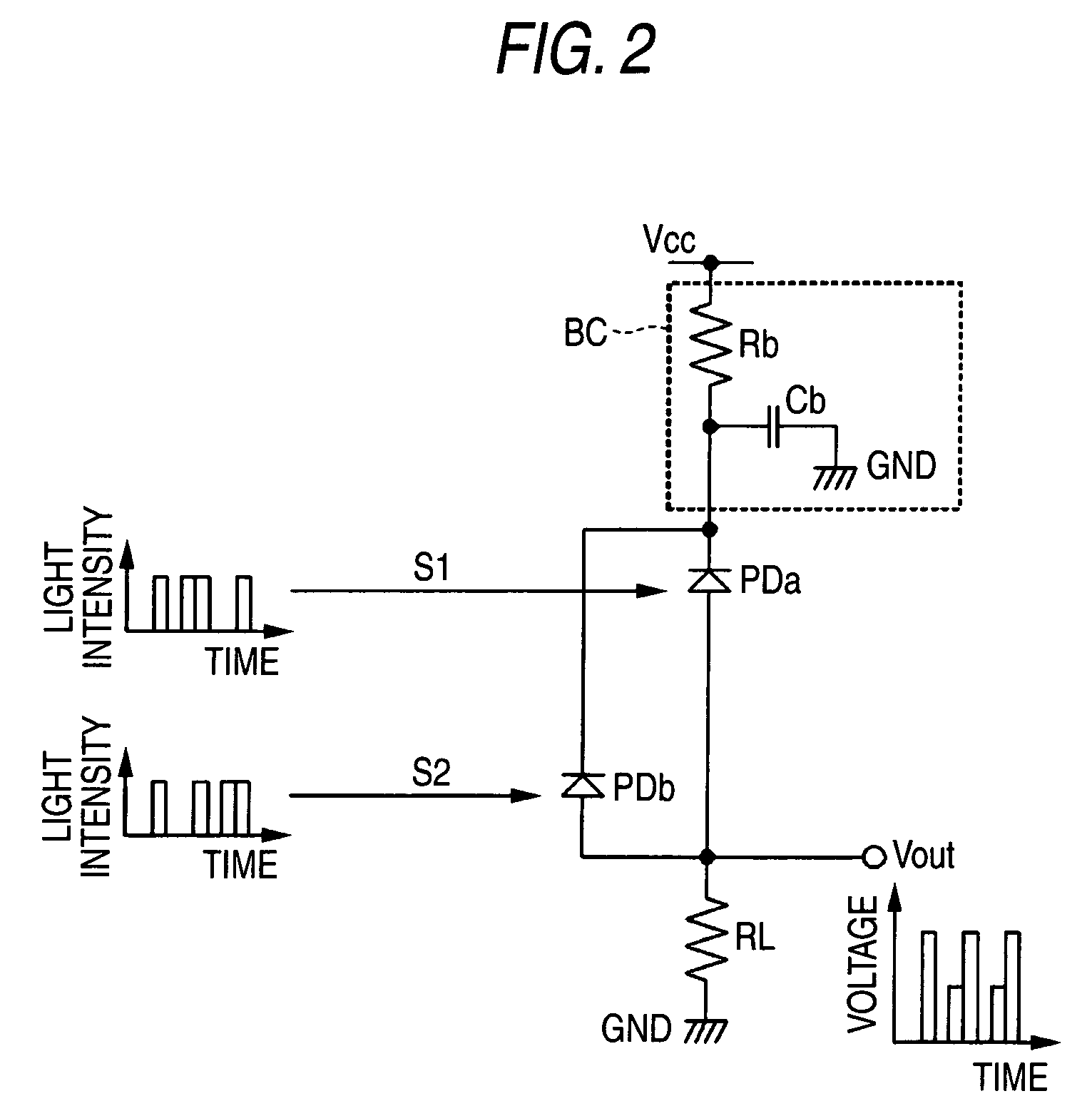
[0046]FIGS. 1 and 2 are diagrams illustrating an embodiment of the invention. Further, FIG. 2 is a diagram illustrating the configuration of a photoelectric conversion portion in an optical logic device shown in FIG. 1. Incidentally, constituents, which are the same those shown in FIG. 6, are designated by the same reference characters as those used for designating such constituents in FIG. 6. Thus, the description of such constituents is omitted herein. As shown in FIG. 1, a photoelectric conversion portion 40 is provided therein, instead of the photoelectric conversion portions 20a and 20b. Moreover, a comparator 50 is provided therein, instead of the logic synthesis processing circuit 30.

[0047]The photoelectric conversion portion 40 is provided with two photodiodes PDa and PDb, the number of which is equal to that of input light signals S1 and S2, in parallel with each other. The photoelect...


PUM

PropertyMeasurementUnit
voltageaaaaaaaaaa
timeaaaaaaaaaa
photoelectricaaaaaaaaaa

Abstract

An optical logic device performs a logic operation on a plurality of input light signals. The optical logic device has a photoelectric conversion portion, in which photoreceivers for receiving input light signals are provided in parallel, that outputs an electric signal obtained by adding up outputs of the photoreceivers, and a comparator that compares a voltage level of the electric signal outputted from the photoelectric conversion portion with a predetermined voltage level.

Description

CROSS-REFERENCE TO RELATED APPLICATIONS[0001]This application is based upon and claims the benefit of priority from the prior Japanese Patent Applications No. 2004-060212, filed on Mar. 4, 2004, the entire contents of which are incorporated herein by reference.BACKGROUND OF THE INVENTION [0002]1. Field of the Invention[0003]The present invention relates to an optical logic device which performs a logic operation on a plurality of input light signals, and particularly, to an optical logic device enabled to perform an optical operation on electric signals without performing time base adjustment on the electric signals after input light signals are converted into the electric signals.[0004]2. Description of the Related Art[0005]In optical communication systems, measuring apparatuses for optical communication, optical computers, and so on, logic operations, such as AND-operations, and OR-operations, are performed on multiple input light signals. Hitherto, a photoelectric conversion port...

Claims


Application Information

Patent Timeline
Patent Type & Authority Patents(United States)
IPC IPC(8): H04J4/00H04J14/00G02F3/00H01J40/14H01L27/115H01L27/14H01L31/10H01L31/167H03K19/14
CPCH03K3/42H03K19/14
Inventor WADA, MORIOMIURA, AKIRAYAKIHARA, TSUYOSHISUEHIRO, MASAYUKIHAYASHI, DAISUKEIIO, SHINJIUMEZAWA, TOSHIMASAKUDO, TAKAHIROMOGI, TAKASHIARAKI, SHOUJIROUDOBASHI, MACHIOIKEZAWA, KATSUYA
Owner YOKOGAWA ELECTRIC CORP
Learn More