Methods for multi-modal wafer testing using edge-extended wafer translator

a translator and multi-modal technology, applied in the field of semiconductor test equipment, can solve problems such as and achieve the effect of improving the difficulty of comprehensive functional testing

Active Publication Date: 2008-11-25
SHANGHAI CARSON SEMICON CO LTD
View PDF4 Cites 29 Cited by
  • Summary
  • Abstract
  • Description
  • Claims
  • Application Information

AI Technical Summary

Problems solved by technology

As integrated circuits have become more complex, and their logic gates have become more deeply embedded, comprehensive functional testing has consequently become more difficult because of the tremendous number of states and state transitions needed for exhaustive fault coverage.
Unfortunately, conventional testing apparatus and methods result in such separate tests being performed sequentially, and often with different physical arrangements of test apparatus.

Method used


Image

  • Methods for multi-modal wafer testing using edge-extended wafer translator
  • Methods for multi-modal wafer testing using edge-extended wafer translator
  • Methods for multi-modal wafer testing using edge-extended wafer translator

Examples


Embodiment Construction

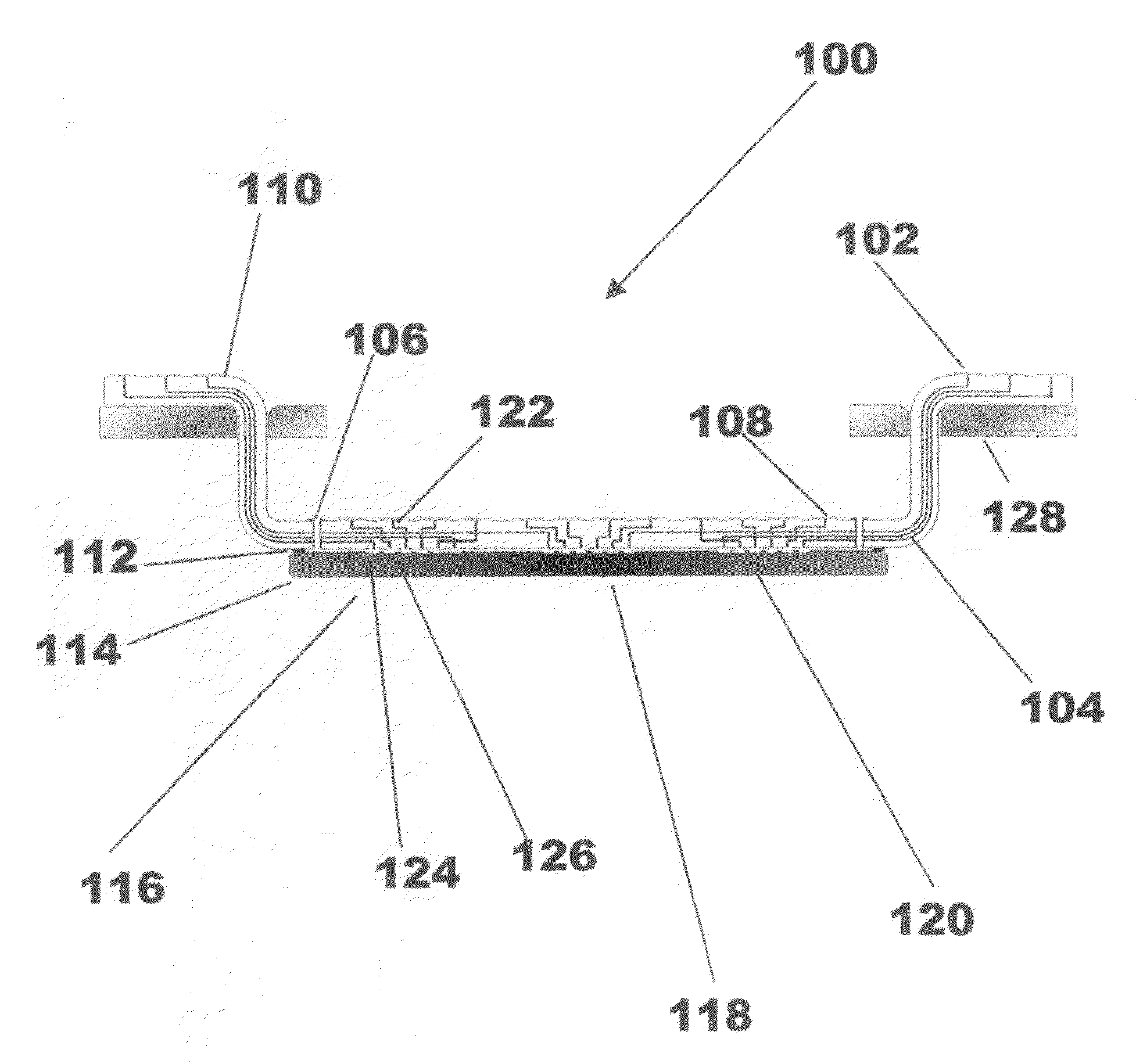
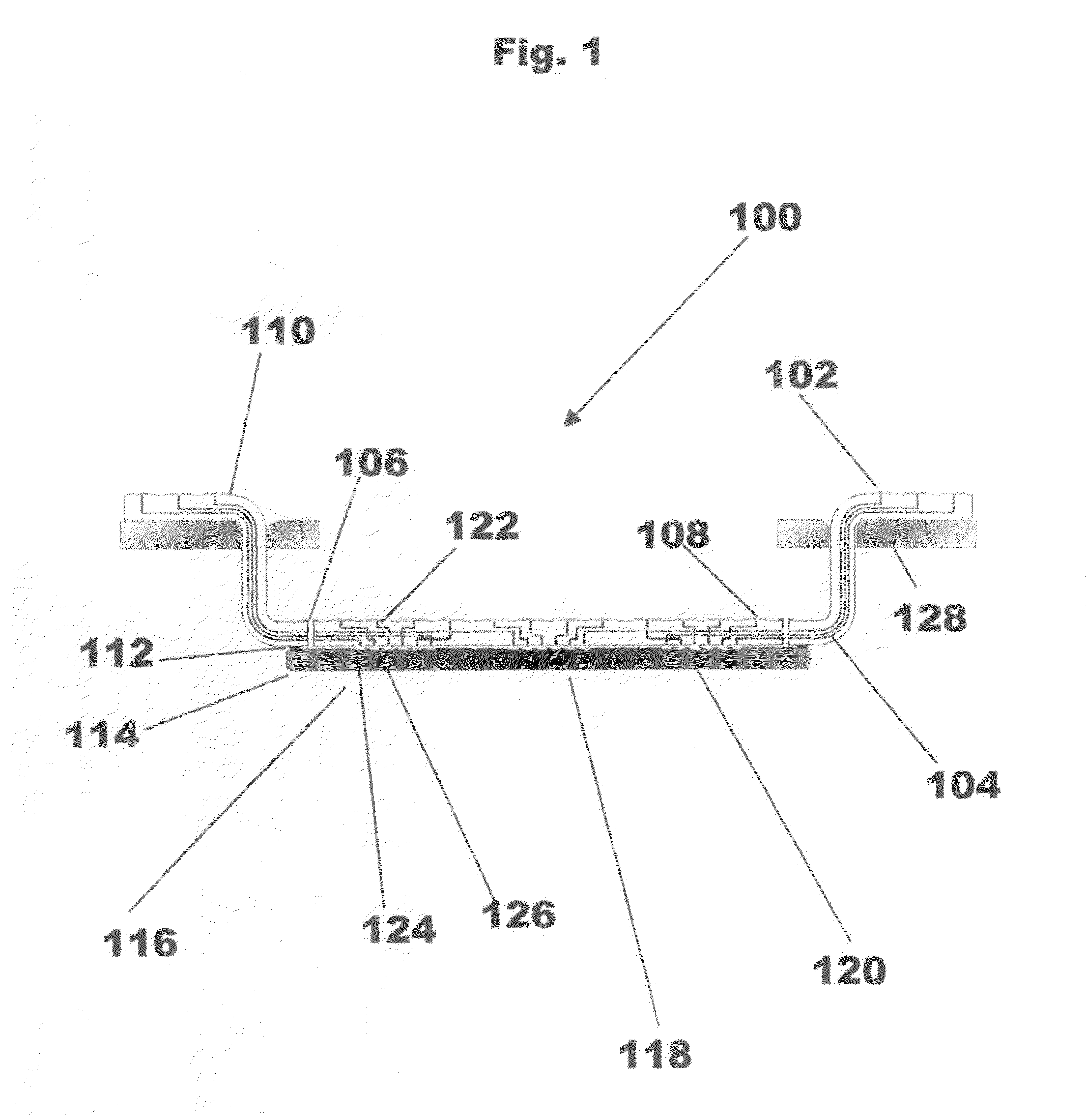
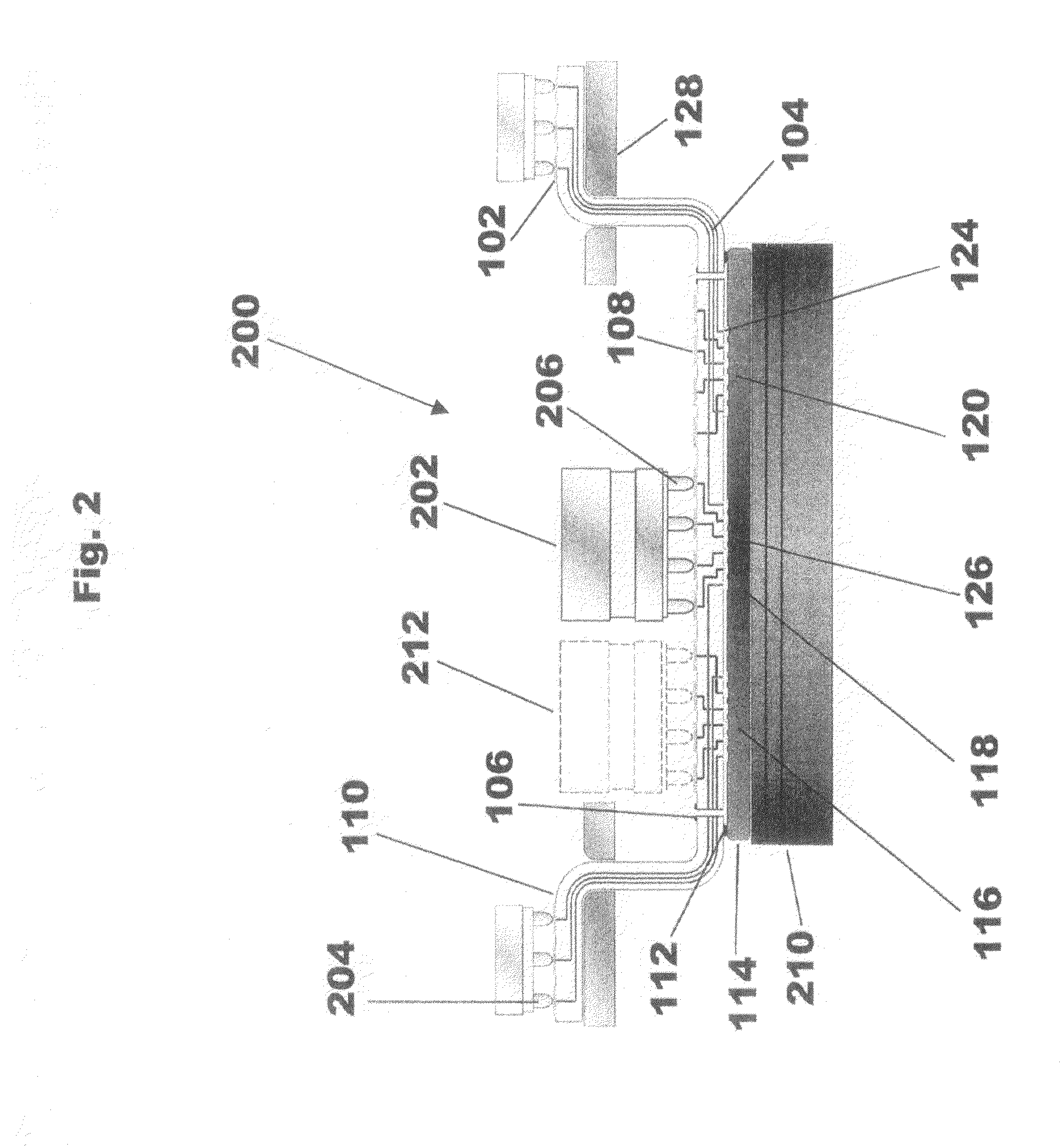
[0016]Generally, embodiments of the present invention provide a means of conducting two or more wafer-level tests under a variety of conditions, either simultaneously, contemporaneously or asynchronously, on a wafer mounted within a single test apparatus. By providing an edge-extended wafer translator, various embodiments of the present invention allow electrical communication with integrated circuits on a wafer through a probe card / wafer prober, and at the same time through an additional set of contact terminals disposed on the wafer translator in an area outside the circumferential edge of the wafer. In various embodiments of the present invention different tests may be performed through the two sets of connections. For example, the same die may be concurrently subjected to different tests, different die may be concurrently subjected to the same test, or different die may be concurrently subjected to different tests.

[0017]In various embodiments, the edge-extended portion of the ed...


PUM


Abstract

Access to integrated circuits of a wafer for concurrently performing two or more types of testing, is provided by bringing a wafer and an edge-extended wafer translator into an attached state. The edge-extended wafer translator having wafer-side contact terminals and inquiry-side contact terminals disposed thereon, a first set of wafer-side contact terminals being electrically coupled to a first set of inquiry-side contact terminals, and a second set of wafer-side contact terminals being electrically coupled to a second set of inquiry-side contact terminals. The edge-extended wafer translator having a central portion generally coextensive with the attached wafer, and an edge-extended portion extending beyond the boundary generally defined by the outer circumferential edge of the wafer. A first set of pads of at least one integrated circuit is electrically coupled to the first set of wafer-side contact terminals, and a second set of pads of the integrated circuit is electrically coupled to the second set of wafer-side contact terminals. The edge-extended wafer translator may be shaped such that its edge-extended portion is not coplanar with the central portion thereof.

Description

CROSS-REFERENCE TO RELATED APPLICATIONS[0001]This non-provisional application claims the benefit of provisional application 60 / 811,585, filed 6 Jun. 2006, and entitled “Methods And Apparatus For Bimodal Wafer Testing”, the entirety of which is hereby incorporated by reference.FIELD OF THE INVENTION[0002]The present invention relates generally to semiconductor test equipment, and more particularly relates to methods and apparatus for wafer sort and wafer DFT / BIST.BACKGROUND[0003]Advances in semiconductor manufacturing technology have resulted in, among other things, reducing the cost of sophisticated electronics to the extent that integrated circuits have become ubiquitous in the modern environment.[0004]As is well-known, it is common to manufacture integrated circuits, on roughly circular semiconductor substrates, or wafers. Further, it is common to form such integrated circuits so that conductive regions disposed on, or close to, the uppermost layers of the integrated circuits are ...

Claims


Application Information

Patent Timeline
Patent Type & Authority Patents(United States)
IPC IPC(8): G01R31/02G01R31/26
CPCG01R1/07342G01R31/2886
Inventor JOHNSON, MORGAN T.
Owner SHANGHAI CARSON SEMICON CO LTD
Why Eureka
Try Eureka