
Organic electroluminescent device

a technology of electroluminescent devices and organic materials, which is applied in the direction of solid-state devices, discharge tubes/lamp details, natural mineral layered products, etc., can solve the problems of device lack of satisfactory luminous efficiency and disadvantageous efficiency of compound energy transfer to dopants

Active Publication Date: 2008-12-23
UDC IRELAND
View PDF7 Cites 11 Cited by
  • Summary
  • Abstract
  • Description
  • Claims
  • Application Information

AI Technical Summary

Problems solved by technology

As described above, condensed-ring aromatic compounds are generally low in the T1 energy level; therefore, the compounds are disadvantageous in efficiency for transferring energy to dopants.
For example, JP-A-2001-167884 (“JP-A” means unexamined published Japanese patent application) discloses an organic electroluminescence device using tetraphenylene, but the device lacks satisfactory luminous efficiency.

Method used


Image

  • Organic electroluminescent device
  • Organic electroluminescent device
  • Organic electroluminescent device

Examples


example 1

[0152]A washed ITO substrate was placed in a depositing apparatus. As a hole transporting material, α-NPD (N,N′-diphenyl-N,N′-di(α-naphthyl)benzidine) was deposited in a thickness of 50 nm on the substrate, then Compound (1-4) and Compound a were co-deposited thereon with a ratio (by mass) of 17:1 in a thickness of 36 nm, followed by depositing Azole compound b thereon in a thickness of 36 nm. A patterned mask (mask providing a light-emitting area of 4 mm×5 mm) was provided on the organic thin layers, and after depositing lithium fluoride in a thickness of about 1 nm in the depositing apparatus, aluminum was deposited in a thickness of about 200 nm thereon, to prepare a luminescent device. A DC constant voltage was applied to the resultant EL device, using Source Measure Unit type 2400 (trade name), manufactured by Toyo Tekunika, to emit light. The luminance of the thus-emitted light was measured, using a luminance meter, BM-8 (trade name) manufactured by Topkon, and the wavelength ...

example 2

[0157]A device was prepared and evaluated in the same manner as in Example 1, except that instead of the Compound (1-4), a mixture of Compound (1-4) and Compound c at a ratio by mass of 1:1 was used. As a result, a green light emission with a chromaticity value of (0.28, 0.62) was obtained. The external quantum efficiency of the device was 12.1%.

[0158]The device durability of this device was evaluated at an initial luminance of 2,000 cd / m2 and a constant current value. As a result, the luminance half time of the device was about 620 hours.

example 3

[0159]A device was prepared and evaluated in the same manner as in Example 1, except that instead of the Compound (1-4), a mixture of Compound (1-4) and Compound d at a ratio by mass of 1:1 was used. As a result, a green light emission with a chromaticity value of (0.28, 0.62) was obtained. The external quantum efficiency of the device was 9.1%.

[0160]The device durability of this device was evaluated at an initial luminance of 2,000 cd / m2 and a constant current value. As a result, the luminance half time of the device was about 780 hours.


PUM

PropertyMeasurementUnit
phosphorescence quantum yieldaaaaaaaaaa

Abstract

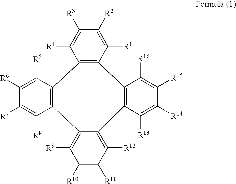
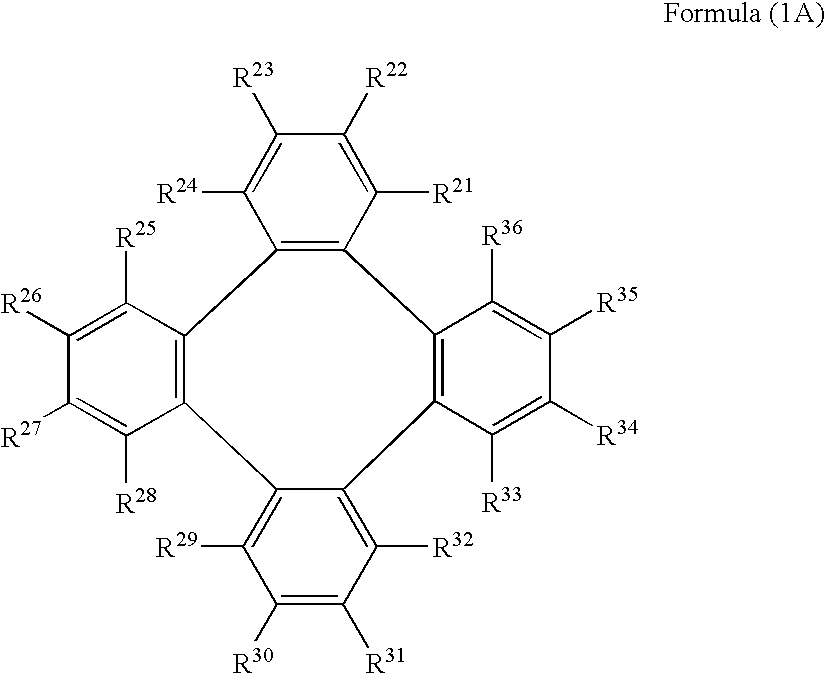
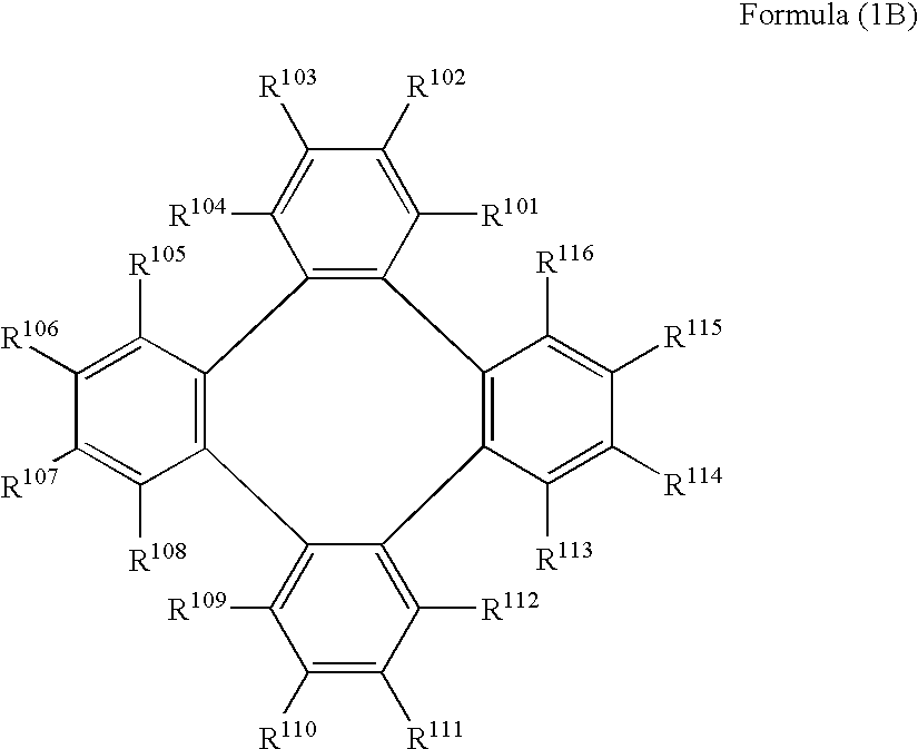
An organic electroluminescent device, which has, between a pair of electrodes, at least one organic layer including a light-emitting layer, in which the organic layer contains a specific tetraphenylene compound, and in which the light-emitting layer contains a phosphorescent material; and a specific tetraphenylene compound that can be used in the device.

Description

FIELD OF THE INVENTION[0001]The present invention relates to an organic electroluminescent device capable of converting electric energy to light, to emit light.BACKGROUND OF THE INVENTION[0002]In these days, research and development are being vigorously made on various display devices. Especially, organic electroluminescent (EL) devices have been noted as promising display devices since they can emit light with a high luminance at a low voltage. Conventional condensed-ring aromatic compounds used in EL devices are chemically stable but low in the lowest triplet excitation energy level (T1). It is therefore desired that organic electroluminescence devices using triplet luminescence be further improved.[0003]As described above, condensed-ring aromatic compounds are generally low in the T1 energy level; therefore, the compounds are disadvantageous in efficiency for transferring energy to dopants. To improve the luminous efficiency, it has been desired to develop aromatic hydrocarbon ma...

Claims


Application Information

Patent Timeline
Patent Type & Authority Patents(United States)
IPC IPC(8): H01L51/54H01L51/50C07C13/62C07C15/20C07C22/08C07C25/22C07C43/275C07C211/54C07C211/61C07C255/52C07C317/14C07D213/24C07D235/14C07D239/26C07D249/08C07D251/16C07D251/24C07D271/10C07D401/10C07D401/14C07D403/10C07D403/14C07D413/14C07D519/00C09K11/06H01L51/00H05B33/14
CPCC07C15/20C07C22/08C07C25/22C07C43/275C07C211/61C07C255/52C07C317/14C07D251/24C07D401/10C07D401/14C07D403/10C07D403/14C07D413/14C09K11/06H01L51/0057H01L51/0058H01L51/0067H01L51/007H01L51/0072H05B33/14C07C2103/24C07C2103/52C07C2103/54C09K2211/1011H01L51/0062H01L51/0077H01L51/0085H01L51/0092H01L51/5016Y10S428/917C07C2603/24C07C2603/52C07C2603/54H10K85/625H10K85/626H10K85/649H10K85/6565H10K85/30H10K85/654H10K85/342H10K85/381H10K85/6572H10K50/11H10K2101/10
Inventor OGASAWARA, JUNIGARASHI, TATSUYASANO, SATOSHI
Owner UDC IRELAND
Learn More