

White organic light emitting device
a light emitting device and organic technology, applied in the field of display devices, can solve the problems of reduced light emission efficiency, low light emission efficiency of light emitting layer, and difficulty in obtaining three uniform primary colors, and achieve the effect of high light emission efficiency and low driving curren
Active Publication Date: 2008-12-04
SAMSUNG DISPLAY CO LTD
View PDF2 Cites 132 Cited by
- Summary
- Abstract
- Description
- Claims
- Application Information
AI Technical Summary
Benefits of technology
[0009]To solve the above and/or other problems, the present invention provides
Problems solved by technology
However, the light emitting layer formed using the first method has reduced light emission efficiency since energy transfer to the dopants is difficult.
However, this produces a light emitting layer with low lig
Method used
View moreImage
Smart ImageViewing Examples

Examples
 PUM
 Abstract
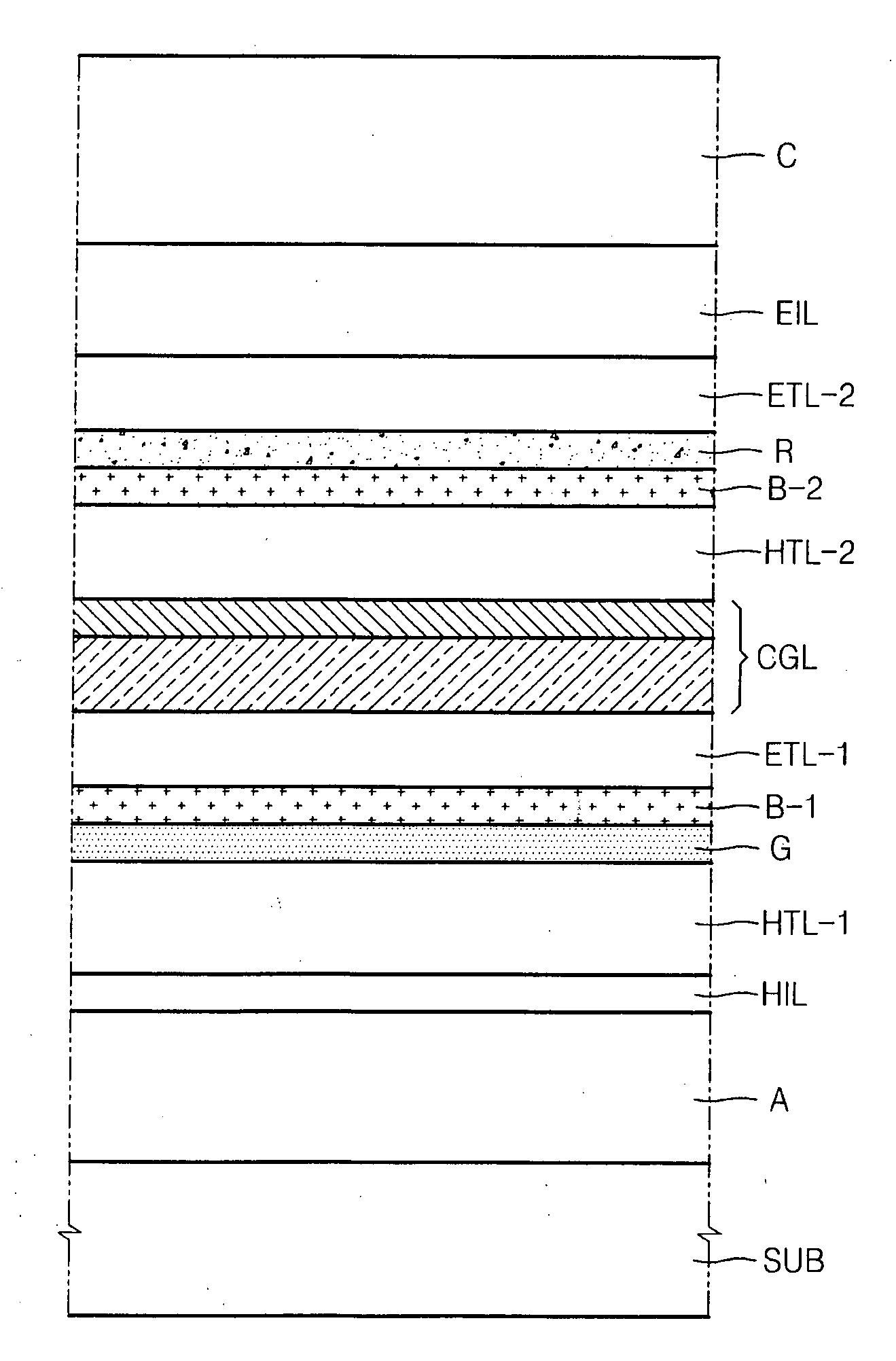
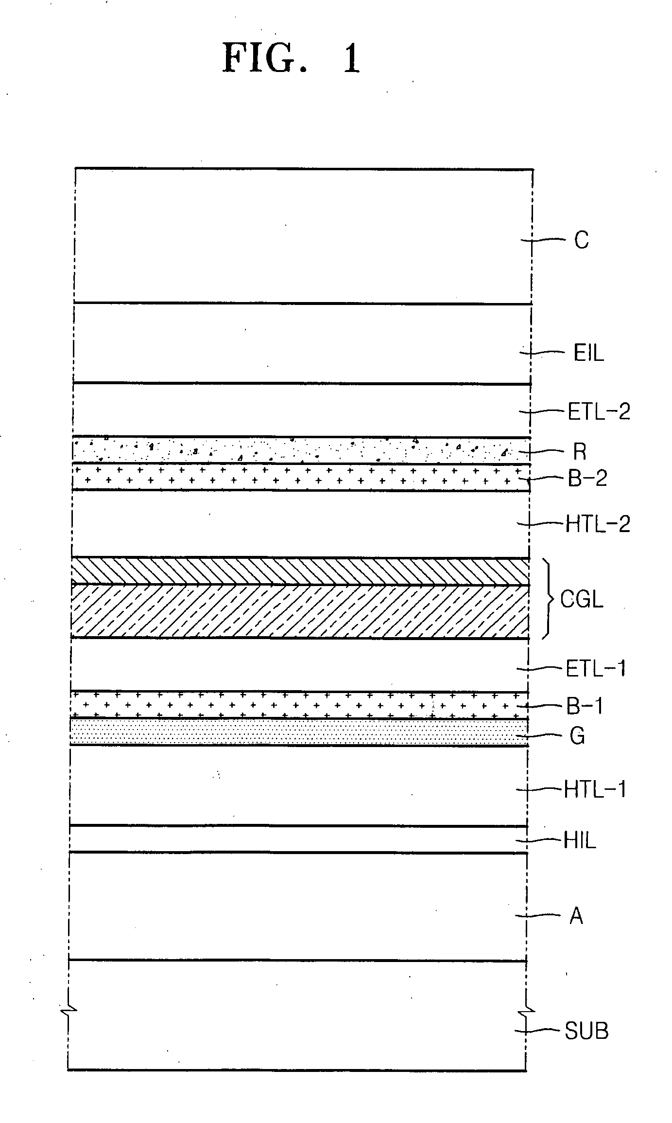
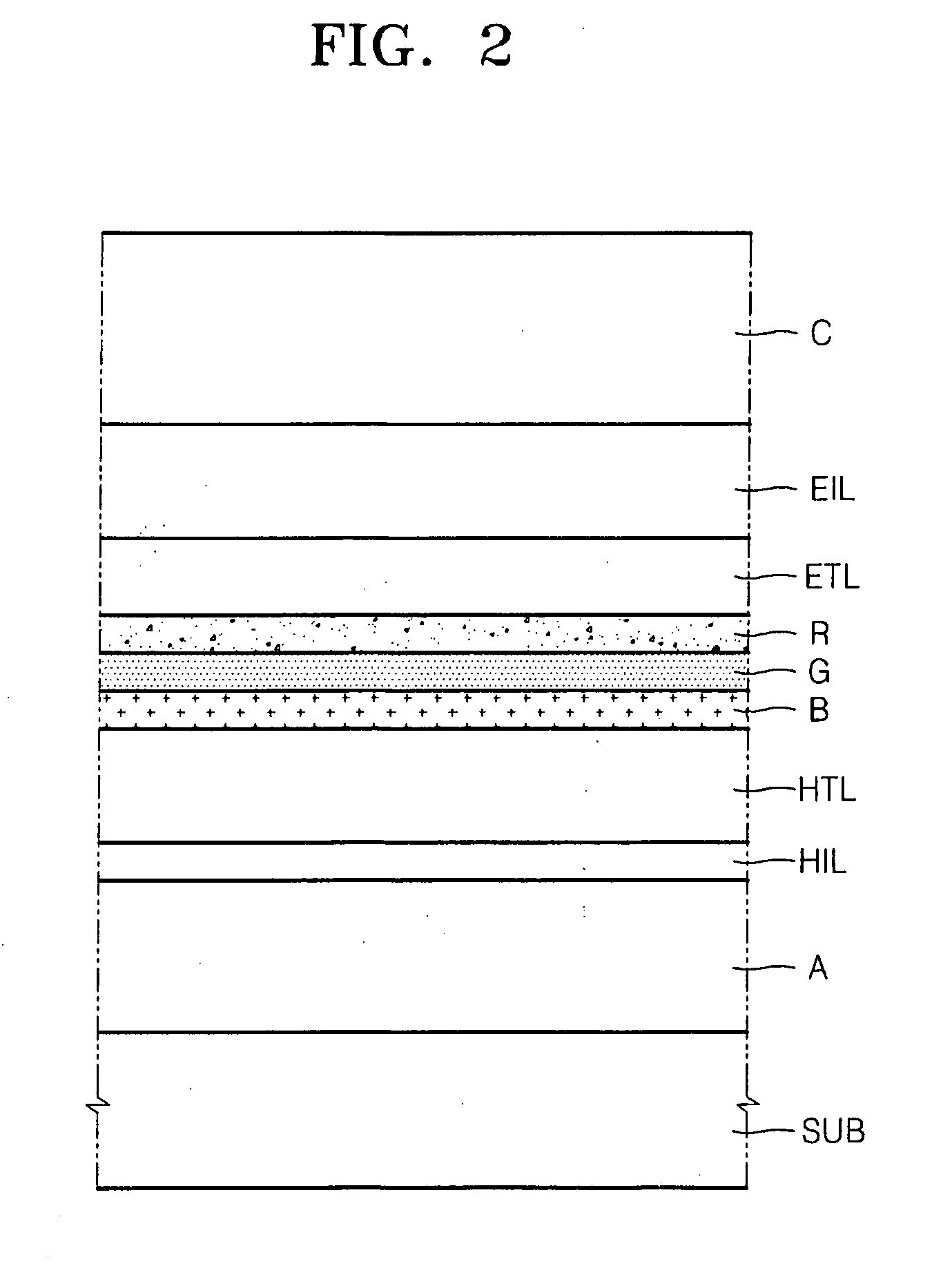
A white organic light emitting device includes an anode, a cathode, a charge generation layer arranged between the anode and the cathode and an organic layer arrangement arranged between the anode and the cathode, the organic layer arrangement including a green light emitting layer, a blue light emitting layer, and a red light emitting layer, one of the green light emitting layer, the blue light emitting layer, and the red light emitting layer includes a first light emitting layer and second light emitting layer, the charge generation layer being arranged between the first light emitting layer and the second light emitting layer.
Description
CLAIM OF PRIORITY[0001]This application makes reference to, incorporates the same herein, and claims all benefits accruing under 35 U.S.C. § 119 from an application for WHITE ORGANIC LIGHT EMITTING DEVICE, earlier filed in the Korean Intellectual Property Office on 31 May 2007 and there duly assigned Serial No. 10-2007-0053472.BACKGROUND OF THE INVENTION[0002]1. Field of the Invention[0003]The present invention relates to a display device, and more particularly, to a white organic light emitting device having high light emission efficiency.[0004]2. Description of the Related Art[0005]Organic light emitting devices (OLEDs) are self emissive display devices that use light generated by combining electrons and holes supplied to a fluorescence or phosphorescence organic compound thin film (hereinafter, an organic thin film). Generally, an OLED has a structure in which an anode, a hole transporting layer, a light emitting layer, an electron transporting layer, and a cathode are sequential...
Claims
Login to View More Application Information
Patent Timeline
 IPC IPC(8): H01J1/62
CPCC09K11/06H01L51/5036H01L27/3209H05B33/14H01L51/5278H10K59/32H10K50/125H10K50/19
InventorNOH, TAE-YONGTAMURA, SHINICHIROCHOI, BYOUNG-KIKIM, MYEONG-SUKKIM, YU-JINHAN, EUN-SIL
OwnerSAMSUNG DISPLAY CO LTD