LED substrate and LED

a technology of led substrate and led light, which is applied in the direction of basic electric elements, electrical equipment, semiconductor devices, etc., can solve the problem that the photon generated in the active region cannot be 100% propagated to the external environment, and achieve the effect of high light emission efficiency

Inactive Publication Date: 2012-11-22
SINO AMERICAN SILICON PROD
View PDF1 Cites 16 Cited by
  • Summary
  • Abstract
  • Description
  • Claims
  • Application Information

AI Technical Summary

Benefits of technology

[0008]The invention is directed to a light emitting diode (LED) substrate, which has high light emitting efficiency.

Problems solved by technology

However, the photons generated in the active region cannot be propagated to external by 100% due to various depletion mechanisms.

Method used


Image

  • LED substrate and LED
  • LED substrate and LED
  • LED substrate and LED

Examples


Embodiment Construction

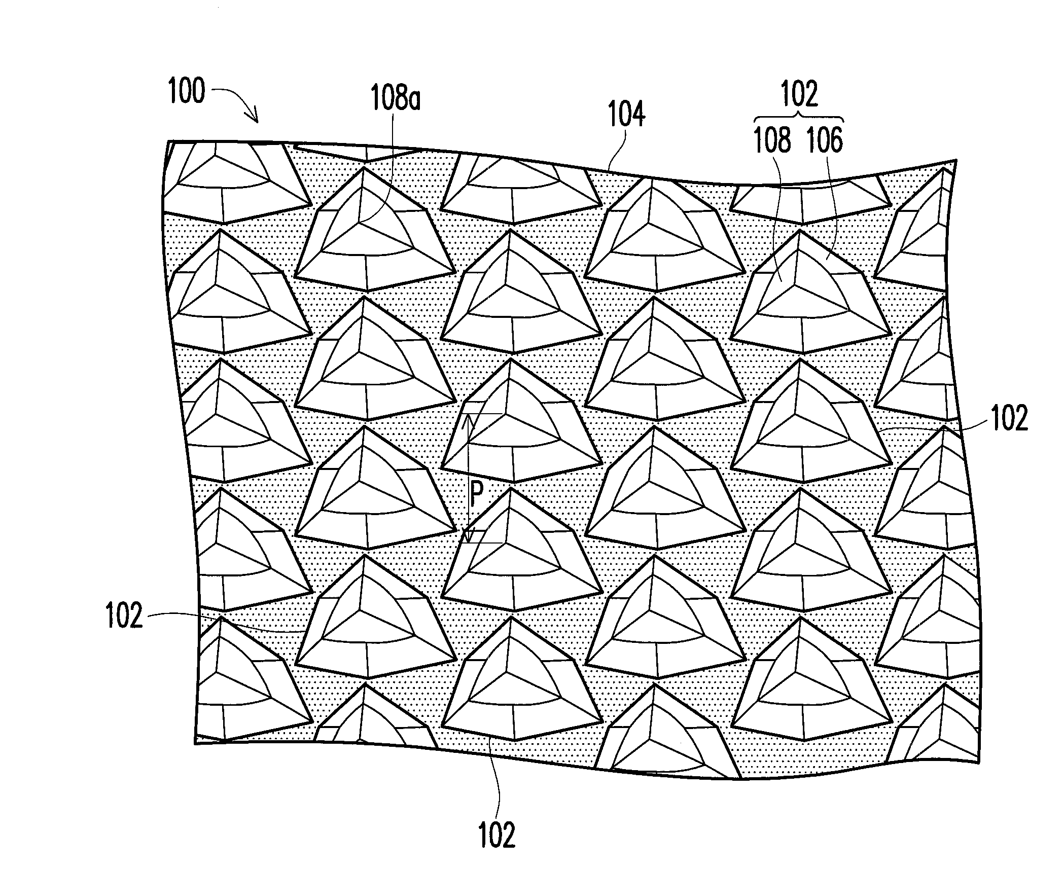
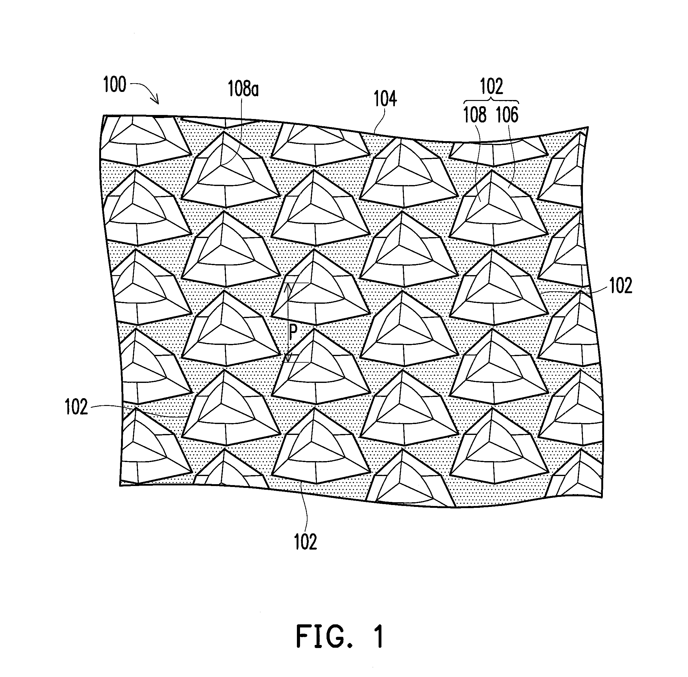
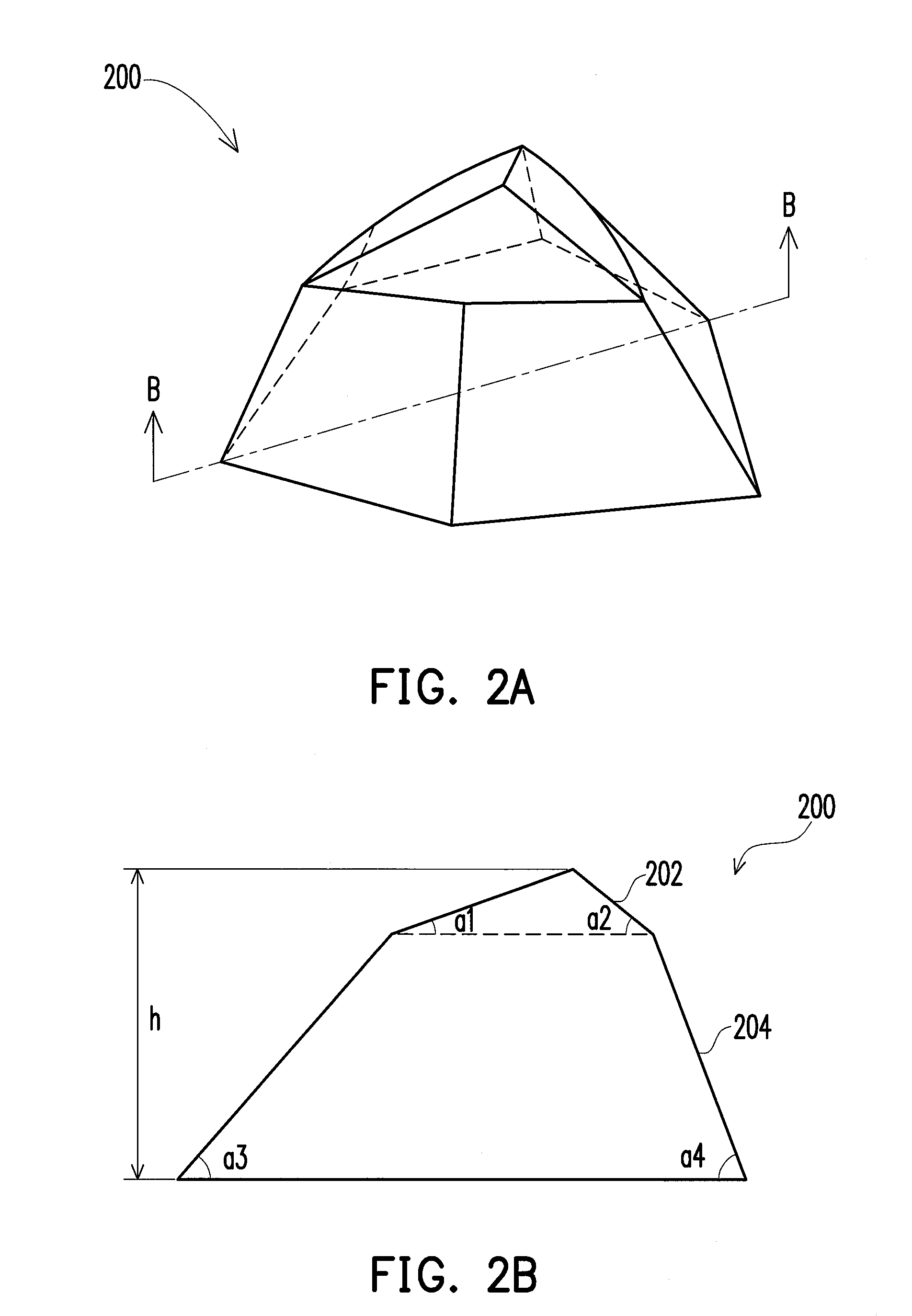
[0034]FIG. 1 is a three-dimensional view of a light emitting diode (LED) substrate according to a first embodiment of the invention. In FIG. 1, a sapphire substrate 100 is illustrated. The sapphire substrate 100 includes a surface 104 consisting of a plurality of upper trigonal and lower hexagonal tapers 102, where each of the upper trigonal and lower hexagonal tapers 102 is consisted of a hexagonal taper 106 and a trigonal taper 108 on the hexagonal taper 106, and a pitch P of the upper trigonal and lower hexagonal tapers 102 is less than 10 μm, which is preferably between 1 μm and 4 μm. The so-called “pitch” refers to a distance between two adjacent upper trigonal and lower hexagonal tapers 102.

[0035]In FIG. 1, a top 108a of the trigonal taper 108 is a pointed end. However, the invention is not limited thereto, and the top 108a of the trigonal taper 108 can also be a platform surface, though the pointed end may have better light emitting efficiency. For example, the surface 104 of...


PUM


Abstract

A light emitting diode (LED) substrate including a sapphire substrate is provided. The sapphire substrate has a surface consisting of a plurality of upper trigonal and lower hexagonal tapers, wherein each of the upper trigonal and lower hexagonal tapers is consisted of a hexagonal taper and a trigonal taper on the hexagonal taper, and a pitch of the upper trigonal and lower hexagonal tapers is less than 10 μm. This LED substrate has high light-emitting efficiency.

Description

CROSS-REFERENCE TO RELATED APPLICATION[0001]This application claims the priority benefit of Taiwan application serial no. 100117040, filed May 16, 2011. The entirety of the above-mentioned patent application is hereby incorporated by reference herein and made a part of this specification.BACKGROUND OF THE INVENTION[0002]1. Field of the Invention[0003]The invention relates to a light emitting diode (LED) substrate. Particularly, the invention relates to a LED substrate having high light extraction efficiency and an LED using the same.[0004]2. Description of Related Art[0005]LED is a light-emitting device fabricated by a compound semiconductor, in which electric energy can be converted into light through combination of electrons and holes. The LED is belonged to a cold light source, and has advantages of low power consumption, none warm up time, long service life and fast response speed, etc., and further has features of high impact resistance and suitable for mass production, and con...

Claims


Application Information

Patent Timeline
Patent Type & Authority Applications(United States)
IPC IPC(8): H01L33/22H01L33/30
CPCH01L33/32H01L33/007H01L33/20H01L33/22
Inventor WU, YEW-CHUNG SERMONHSIAO, FENG-CHINGCHEN, YU-CHUNGTSENG, BO-HSIANGLIN, BO-WENPENG, CHUN-YENHSU, WEN-CHING
Owner SINO AMERICAN SILICON PROD
Why Eureka
Try Eureka