Graded vias for LED chip P- and N- contacts

Active Publication Date: 2016-08-09
CREELED INC
View PDF2 Cites 23 Cited by
  • Summary
  • Abstract
  • Description
  • Claims
  • Application Information

AI Technical Summary

Benefits of technology

[0017]Additionally, the chip includes a plurality of non-uniform vias providing an electrical path to one of the oppositely doped la

Problems solved by technology

For conventional LEDs with a single out-coupling surface, the external quantum efficiency can be limited by total internal reflection (TIR) of light from the LED's emission region.
Emission inefficiencies may also be caused by poor output uniformity and/or current crowding.
While the reflective cup 13 may direct light in an upward directio

Method used


Image

  • Graded vias for LED chip P- and N- contacts
  • Graded vias for LED chip P- and N- contacts
  • Graded vias for LED chip P- and N- contacts

Examples


Embodiment Construction

[0038]Embodiments of the present invention provide improved light emitting devices and packages and methods for fabricating the same, wherein the improvements may allow for improved efficiency and uniformity.

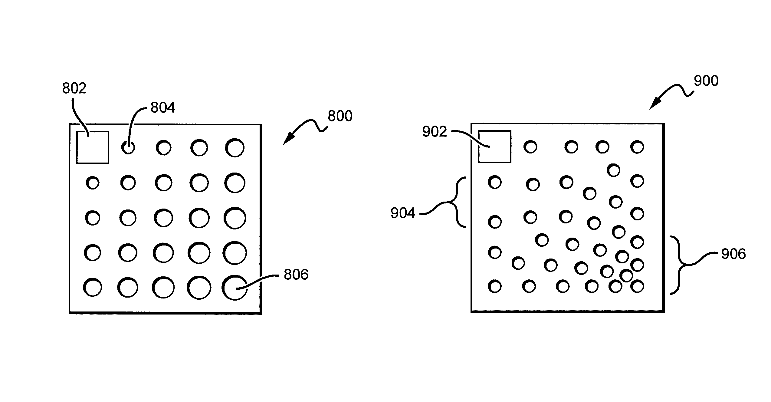
[0039]The present disclosure will now set forth detailed descriptions of various embodiments. These embodiments provide methods and devices pertaining to solid state devices, such as light emitting devices, various light emitters, LED chips, LED wafers, LED components, and methods of manufacture thereof. Embodiments incorporating features of the present disclosure allow for the creation of devices with efficient or improved light emission or output. These embodiments may incorporate improved current spreading structures, such as non-uniform via structures or varied via structures. Some embodiments of this disclosure may also refer to contact pad placement to improve current flow.

[0040]Different embodiments of light emitting diode (LED) chips according to the present disclosure c...


PUM


Abstract

The present disclosure provides various embodiments of light emitting chips and packages with improved current spreading structures, such as non-uniform via structures or varied via structures. In some embodiments, these structures may be used to regulate current flow and current crowding in order to improve emitter efficiency and uniformity. Some embodiments of this disclosure may also refer to contact pad placement to improve current flow. In some embodiments of non-uniform via structures, the size of the vias may vary, whereas in other embodiments, the shape or spacing between the vias may vary.

Description

BACKGROUND OF THE INVENTION[0001]1. Field of the Invention[0002]This invention relates to light emitting diode (LED) chips and in particular to LED chips with graded or varied via sizes to control current flow.[0003]2. Description of the Related Art[0004]Light emitting diodes (LED or LEDs) are solid state devices that convert electric energy to light, and generally comprise one or more active layers of semiconductor material sandwiched between oppositely doped layers. When a bias is applied across the doped layers, holes and electrons are injected into the active layer where they recombine to generate light. Light is emitted from the active layer and from all surfaces of the LED.[0005]For typical LEDs it is desirable to operate at the highest light emission efficiency, and one way emission efficiency can be measured is by the emission intensity in relation to the input power, or lumens per watt. One way to maximize emission efficiency is by maximizing extraction of light emitted by ...

Claims


Application Information

Patent Timeline
IPC IPC(8): H01L31/0256H01L33/08H01L33/38
CPCH01L33/382H01L33/08H01L33/14H01L2224/48091H01L2924/00014
Inventor PLACE, THOMASLANGSDORF, BENNETT DEAN
Owner CREELED INC
Why Eureka
Try Eureka