Silicon-based light-emitting device and preparation method thereof

A light-emitting device, silicon-based technology, applied in the direction of semiconductor devices, electrical components, circuits, etc., can solve the problem that the carrier injection efficiency device light extraction efficiency needs to be improved, the polystyrene microspheres are not strong in etching resistance, and cannot Constrain light lateral scattering and other issues to achieve the effect of facilitating industrialization links and promotion, increasing light extraction efficiency, and improving light extraction efficiency

Inactive Publication Date: 2011-12-14
SUZHOU INST OF NANO TECH & NANO BIONICS CHINESE ACEDEMY OF SCI
View PDF5 Cites 17 Cited by
  • Summary
  • Abstract
  • Description
  • Claims
  • Application Information

AI Technical Summary

Problems solved by technology

The invention patent intends to enhance the field emission effect with the rough surface of silicon cones in an array, but because the etching resistance of polystyrene microspheres is not strong, and plasma etching is used, the length of the obtained silicon cones is very large. Limitation, the lateral scattering of light cannot be well restricted, so that the injection efficiency of carriers and the light extraction efficiency of the device still need to be improved

Method used


Image

  • Silicon-based light-emitting device and preparation method thereof
  • Silicon-based light-emitting device and preparation method thereof
  • Silicon-based light-emitting device and preparation method thereof

Examples


preparation example Construction

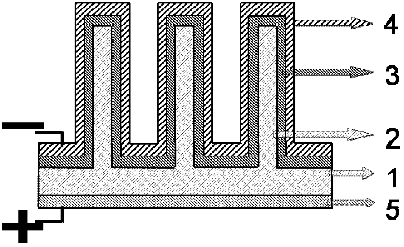
[0038] The method for preparing the aforementioned silicon-based light-emitting device may include the following process steps:

[0039] (1) Clean the heavily doped (for example, B heavily doped) P-type silicon wafers with a resistivity of and 0.004-0.005Ω·cm;

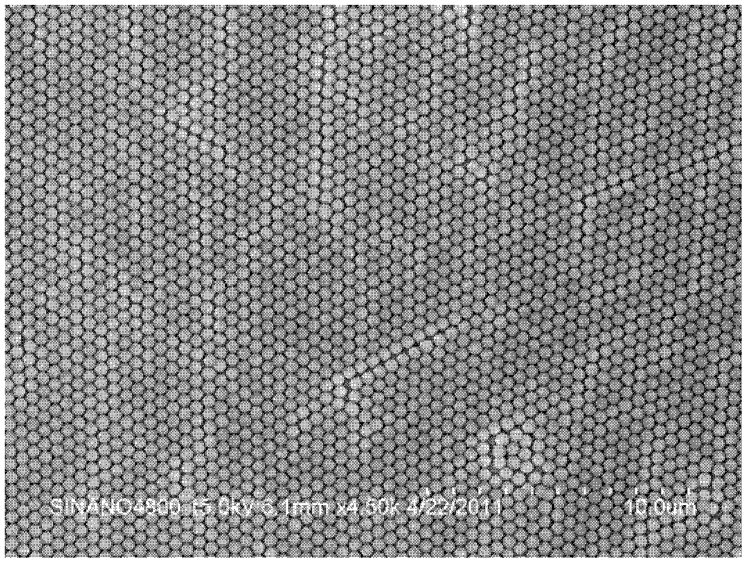
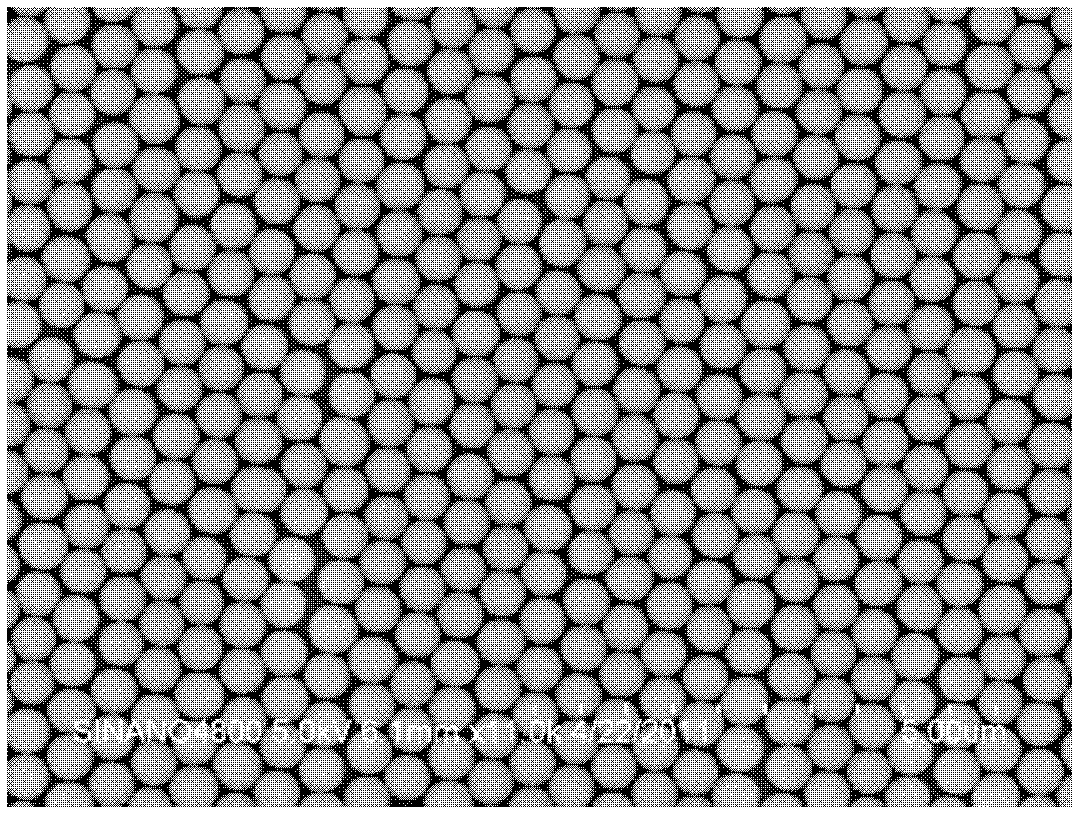
[0040] (2) Self-assembly of microspheres to form large-area and less-defect two-dimensional ordered SiO by pulling method 2 Nano microsphere monolayer colloidal layer;

[0041] (3) Using microsphere mask etching technology to obtain silicon nanopillar photonic crystal arrays through deep reactive ion etching;

[0042] (4) Using PECVD or LPCVD and subsequent annealing process to conformally grow a thin film layer containing nano-silicon quantum dot structure;

[0043] (5) Conformal growth of transparent electrodes;

[0044] (6) Deposition of back ohmic electrode on silicon substrate.

[0045] The above-mentioned pulling method is similar to the LB film method, and can be adjusted by adjusting the SiO 2The particle...


PUM


Abstract

The invention discloses a silicon-based light-emitting device and a preparation method thereof. The device includes a silicon substrate, the front of the substrate is etched to form a nano-column photonic crystal array, and a film layer containing a silicon nanocrystal quantum dot structure is conformally deposited on the array, and the film layer is covered with a transparent conformal electrode. Ohmic contact electrodes are deposited on the bottom and back; the method is as follows: using microsphere mask etching technology on the front of the substrate to obtain a silicon nanocolumn photonic crystal array through deep reactive ion etching, and then co-existing on the silicon nanocolumn photonic crystal array. Formally grow a thin film layer containing a nano-silicon quantum dot structure and a transparent conformal electrode, and deposit an ohmic contact electrode on the back of the substrate to obtain the target product. The silicon-based light-emitting device of the present invention adopts photonic crystal nano-column array and silicon nano-crystal quantum dot structure at the same time, which effectively improves the light extraction efficiency and carrier injection efficiency, thereby improving the luminous intensity and light emission efficiency of the device, and the device structure is simple, The process is simple and the cost is low.

Description

technical field [0001] The invention particularly relates to a silicon-based light-emitting device and a preparation method thereof, belonging to the technical field of semiconductor optoelectronic devices. Background technique [0002] The realization of optical gain and even lasing in silicon materials has always been a goal that the microelectronics industry has been paying close attention to and trying to achieve. From the silicon laser developed by Intel Corporation using the Raman effect to the lasing behavior observed by Brown University on the introduction of A-center defects on SOI chips, many scientific research institutions are committed to the research of silicon-based light sources and lasers. However, due to the indirect bandgap structure of the silicon material itself, its luminous efficiency is still relatively low. Most of the current semiconductor light-emitting devices are made of non-silicon-based materials, which are not compatible with the current matu...

Claims


Application Information

Patent Timeline
Patent Type & Authority Applications(China)
IPC IPC(8): H01L33/02H01L33/20H01L33/00
Inventor 李永垒钱波蒋春萍王亦
Owner SUZHOU INST OF NANO TECH & NANO BIONICS CHINESE ACEDEMY OF SCI
Why Eureka
Try Eureka