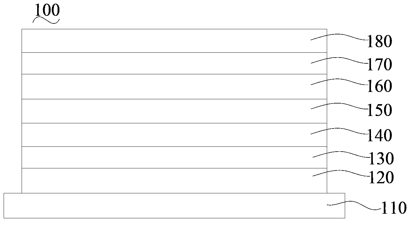
Top emission organic light-emitting device and manufacturing method thereof
A luminescence and top-emission technology, applied in the direction of organic semiconductor devices, electric solid devices, chemical instruments and methods, etc., can solve problems such as unfavorable light efficiency, insufficient transmittance, unbalanced carrier injection, etc., and achieve improved Injection efficiency, high light efficiency, the effect of realizing light effect
- Summary
- Abstract
- Description
- Claims
- Application Information
AI Technical Summary
Problems solved by technology
Method used
Image

Examples
preparation example Construction
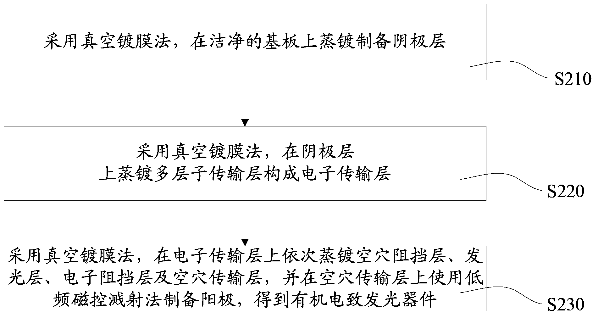
[0033] like figure 2 As shown, this embodiment also provides a method for preparing a top-emitting organic electroluminescent device, including the following steps:
[0034] In step S210, a cathode layer is prepared by vapor deposition on a clean substrate by using a vacuum coating method.
[0035] Before use, the substrate can be ultrasonically cleaned in deionized water containing detergent. After cleaning, it is treated with isopropanol and acetone in ultrasonic for 20 minutes, and then dried with nitrogen to form a clean substrate.
[0036] In step S220, a vacuum coating method is used to vapor-deposit multiple sub-transport layers on the cathode layer to form an electron transport layer. Wherein, the material of each sub-transport layer includes a host material and a doping material doped in the host material, and the host material is 2-(4-biphenyl)-5-(4-tert-butyl)phenyl-1 ,3,4-oxadiazole, (8-hydroxyquinoline)-aluminum, 4,7-diphenyl-phenanthroline, 1,3,5-tris(1-phenyl...
Embodiment 1
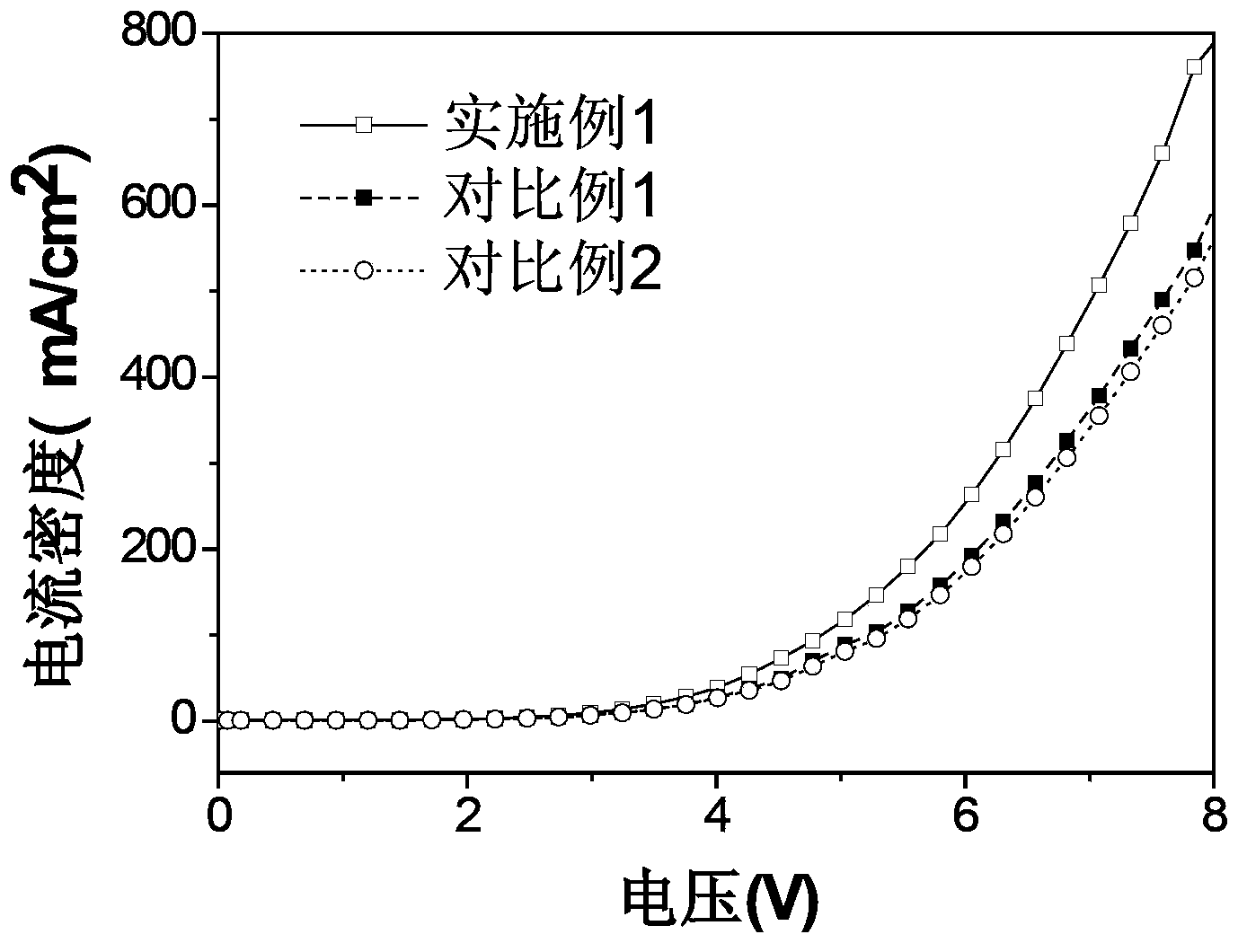
[0042] The structure of the top emission organic electroluminescence device of the present embodiment is: glass substrate / Ag / (CsN 3 :Bphen(20%) / CsN 3 :Bphen(15%) / CsN 3 :Bphen(10%) / CsN 3 :Bphen(5%)) / BAlq / Ir(MDQ) 2 (acac): NPB(5%) / TAPC / CuPc / ITO, where ":" in the corresponding layer indicates doping, the percentage data in brackets indicates the doping mass percentage of the former in the corresponding layer, " / " indicates stacking, Concrete preparation process is as follows:
[0043] The glass substrate is placed in deionized water containing detergent for ultrasonic cleaning, and after cleaning, it is treated with isopropanol and acetone in ultrasonic for 20 minutes, and then dried with nitrogen to obtain a clean glass substrate.
[0044] The Ag cathode layer with a thickness of 100nm was prepared by vapor deposition on the surface of a clean glass substrate by vacuum coating method.
[0045] An electron transport layer including four sub-transport layers was prepared by v...
Embodiment 2
[0049] The structure of the top emission organic electroluminescence device of the present embodiment is: glass substrate / Ag / (LiN 3 :TPBi(15%) / LiN 3 :TPBi(12%) / LiN 3 :TPBi(8%) / LiN 3 :TPBi(5%) / LiN 3 :TPBi(1%)) / BAlq / DCJTB: Alq 3 (1%) / TAPC / CuPc / ITO, where ":" in the corresponding layer indicates doping, the percentage data in brackets indicates the doping mass percentage of the former in the corresponding layer, " / " indicates stacking, and the specific preparation process is as follows:
[0050] The glass substrate is placed in deionized water containing detergent for ultrasonic cleaning, and after cleaning, it is treated with isopropanol and acetone in ultrasonic for 20 minutes, and then dried with nitrogen to obtain a clean glass substrate.
[0051] The Ag cathode layer with a thickness of 100nm was prepared by vapor deposition on the surface of a clean glass substrate by vacuum coating method.
[0052] An electron transport layer composed of five sub-transport layers was ...
PUM
| Property | Measurement | Unit |
|---|---|---|
| thickness | aaaaa | aaaaa |
| thickness | aaaaa | aaaaa |
| thickness | aaaaa | aaaaa |
Abstract
Description
Claims
Application Information
 - R&D
- Intellectual Property
- Life Sciences
- Materials
- Tech Scout
- Unparalleled Data Quality
- Higher Quality Content
- 60% Fewer Hallucinations
Browse by: Latest US Patents, China's latest patents, Technical Efficacy Thesaurus, Application Domain, Technology Topic, Popular Technical Reports.
© 2025 PatSnap. All rights reserved.Legal|Privacy policy|Modern Slavery Act Transparency Statement|Sitemap|About US| Contact US: help@patsnap.com