Manufacturing method of GaN-based LED by annealing to strip and inverse SiC substrate

A manufacturing method and substrate technology, applied in the field of optoelectronics, can solve the problems of less than 50% front light extraction efficiency, inability to adopt flip-chip structure of LED, low power, etc., and achieve the effect of solving low light extraction efficiency

Active Publication Date: 2011-08-10
航天智讯新能源(山东)有限公司
View PDF2 Cites 0 Cited by
  • Summary
  • Abstract
  • Description
  • Claims
  • Application Information

AI Technical Summary

Problems solved by technology

[0012] The present invention aims at the problems of low reliability, low power, less than 50% front light output efficiency, and inability to adopt flip-chip structure for LEDs on SiC substrates in the existing production of LEDs based on SiC or Si substrates, etc., and provides a Fabrication method of annealing and stripping flip-chip GaN-based LEDs from SiC substrates capable of improving luminous intensity

Method used


Image

  • Manufacturing method of GaN-based LED by annealing to strip and inverse SiC substrate
  • Manufacturing method of GaN-based LED by annealing to strip and inverse SiC substrate
  • Manufacturing method of GaN-based LED by annealing to strip and inverse SiC substrate

Examples


Embodiment Construction

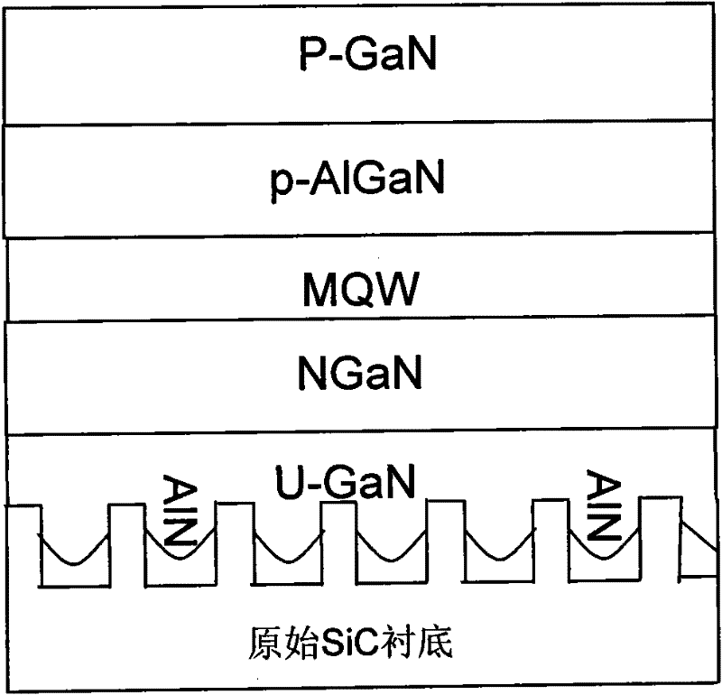
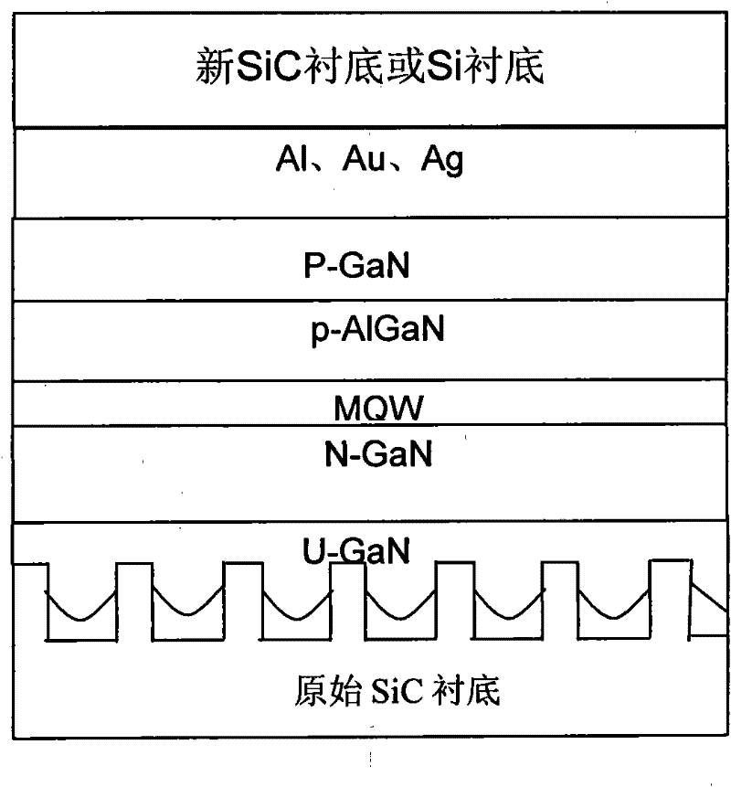
[0028] The manufacturing method of the flip-chip SiC substrate GaN-based LED of the present invention utilizes a graphic substrate and annealing stripping, and the specific manufacturing process is as follows:

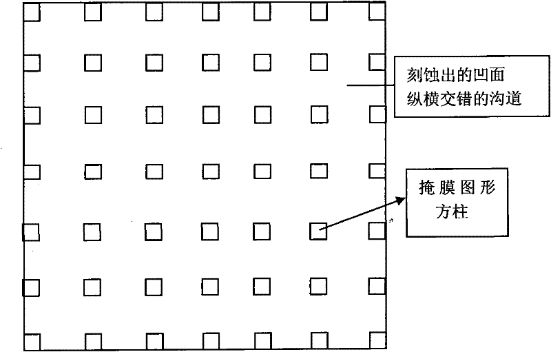
[0029] 1 Fabrication of the original SiC pattern substrate by dry etching

[0030] (1) Evaporate a layer of thickness on the original SiC substrate SiO 2 As a mask, the SiO 2 Coat the photoresist on the mask, pass the pre-engraved pattern mask on the photoresist, and use the photolithography machine to expose and carve the required mask pattern (that is, the place outside the pattern mask protection is exposed).

[0031] (2) Then put it into a 0.5%-5% sodium hydroxide solution for about 10 seconds to 60 seconds to develop, and the photoresist will be removed when developing the place exposed by photolithography, exposing the SiO outside the pattern protection 2 , use HF acid to etch away the SiO exposed on the surface after development 2 , these places expose the ...


PUM


Abstract

The invention provides a manufacturing method of a GaN-based LED by annealing to strip and inverse a SiC substrate. The method comprises the following steps of: (1), etching interlaced channels on the surface of the primary SiC substrate to expose small square columns so as to form a primary SiC pattern substrate; (2), growing epitaxial wafers with conventional structures on the formed primary SiC pattern substrate by a conventional method, wherein the epitaxial wafer comprises a substrate, an AlN buffer layer, an N-type GaN layer, an MQW layer and a P-type GaN layer; (3), plating a layer of reflective metal on the P-type GaN layer on the upper surface of the grown epitaxial wafers, and bonding the reflective metal on a new SiC or Si substrate; and (4), putting the bonded epitaxial wafersin a high-temperature annealing furnace and annealing to strip the primary substrate on the epitaxial wafers. The SiC substrate is successfully inversed and stripped by a method of annealing to stripthe primary substrate due to different thermal expansion coefficients between the SiC substrate and GaN; the light emitting rate is over 90 percent; and the problem of low light emitting efficiency is solved.

Description

technical field [0001] The invention relates to a stripping method of a SiC flip-chip LED that is annealed and stripped from a pattern substrate, and belongs to the field of optoelectronic technology. Background technique [0002] Due to the high power density of the high-power LED chip, the designer and manufacturer of the device must optimize the thermal system of the device in terms of structure and materials. At present, there are two types of GaN-based epitaxial substrate materials: one is sapphire represented by Nichia Chemical of Japan; the other is SiC substrate represented by CREE of the United States. In the traditional sapphire substrate GaN chip structure, the electrodes are just located on the light-emitting surface of the chip. In this structure, a small portion of the p-GaN layer and the "light emitting" layer are etched to make electrical contact with the underlying n-GaN layer. Light is extracted from the topmost p-GaN layer. The limited electrical conduc...

Claims


Application Information

Patent Timeline
Patent Type & Authority Patents(China)
IPC IPC(8): H01L33/00
Inventor 吴德华朱学亮杨鑫沼曲爽李树强王成新徐现刚
Owner 航天智讯新能源(山东)有限公司
Why Eureka
Try Eureka