Laser stripping method using metallic passage beds to transfer GaN substrate

A laser lift-off and transition layer technology, which is applied in the manufacture of electrical components, circuits, semiconductor/solid-state devices, etc., can solve the problems of affecting the current diffusion and output optical power of the device, complex device preparation process, poor thermal conductivity, etc.

Inactive Publication Date: 2008-02-06
XIAMEN UNIV
View PDF0 Cites 9 Cited by
  • Summary
  • Abstract
  • Description
  • Claims
  • Application Information

AI Technical Summary

Problems solved by technology

However, sapphire and GaN have a 16% lattice mismatch, resulting in high-density line dislocations in the epitaxial wafer structure, thereby limiting the quality and thickness of the GaN epitaxial layer (1, Plano W E, MajorJ S, Welch D F.X-ray studies of high quality GaN grown on 0001 sapphire[J]. Electronics Letters, 1994, 30: 2079-2081; 2. Shen X Q, Matsuhata H, Okumura H. Reduction of the threading dislocation density in GaN films grown on victim sapphire (0001) substrates [J].Appl.Phys.Lett., 2005, 86:021912-021914); In addition, Al 2 o 3 The thermal conductivity is poor, and the thermal conductivity is about 0.5W/cm K, which makes the heat dissipation problem of GaN-based devices prominent, especially in hi

Method used


Image

  • Laser stripping method using metallic passage beds to transfer GaN substrate

Examples


Embodiment 1

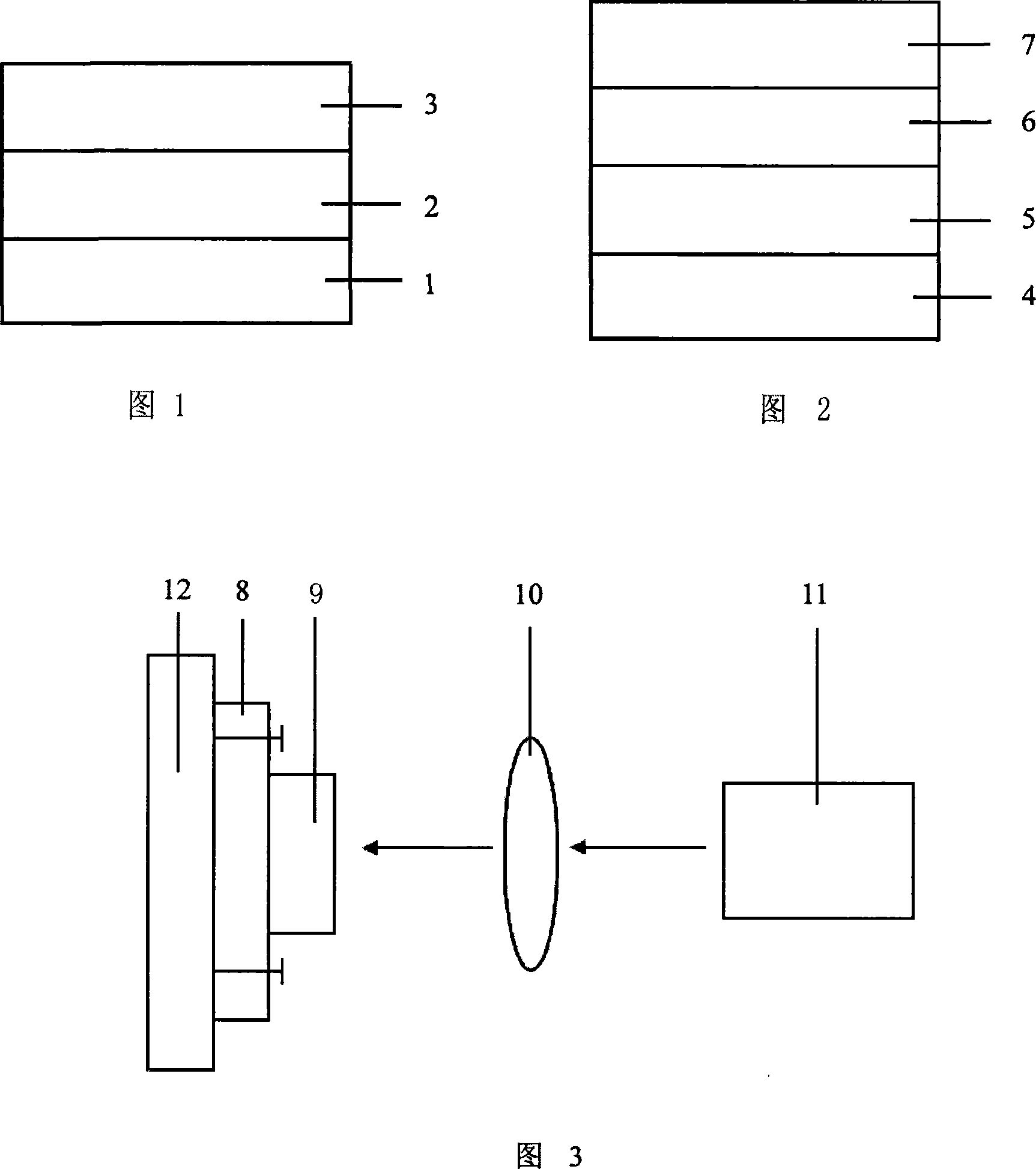
[0026] Referring to FIG. 1, a 40nm Ti layer 2 and a 200nm Au layer 3 are sputtered on a Si(001) substrate 1 in sequence to obtain a silicon wafer sputtered with Ti and Au.

[0027] Referring to FIG. 2, 40 nm Ni6 and 200 nm Au7 were sputtered sequentially on GaN5 with a sapphire substrate 4 to obtain a gallium nitride sheet sputtered with Ni and Au.

[0028] The bonding interfaces of silicon wafers sputtered with Ti and Au and gallium nitride wafers sputtered with Ni and Au are all metals. For the use of GaN-based materials to prepare light-emitting devices, metal multilayer films can also further improve reflectivity .

[0029] The silicon wafer sputtered with Ti and Au and the metal surface of the gallium nitride wafer sputtered with Ni and Au are bonded face-to-face, and then put into the inner cavity of the bonding machine, and the temperature is set to 150° C. for pre-bonding. The introduction of pre-bonding is conducive to the uneven surface of the silicon wafer sputtered wit...

Embodiment 2

[0035] Similar to Embodiment 1, the difference is that a 50nm Ti layer and a 500nm Au layer are sputtered sequentially on a Si(001) substrate to obtain a silicon wafer sputtered with Ti and Au. Sputtering 50nm of Ni and 500nm of Au on the GaN with a sapphire substrate in turn, to obtain a gallium nitride sheet sputtered with Ni and Au. The silicon wafer sputtered with Ti and Au and the metal surface of the gallium nitride wafer sputtered with Ni and Au are bonded face to face, and then put into the inner cavity of the bonding machine, and the temperature is set to 100° C. for pre-bonding. After pre-bonding, the temperature of the bonding machine is increased to 200°C, and the sapphire / gallium nitride / metal layer / silicon bonding wafer structure is formed after 1 hour of constant temperature. The laser energy density of the laser is 200mJ / cm 2 .

Embodiment 3

[0037] Similar to Embodiment 1, the difference is that a 10nm Ti layer and an 80nm Au layer are sequentially sputtered on a Si(001) substrate to obtain a silicon wafer sputtered with Ti and Au. Sputtering 10nm of Ni and 80nm of Au on the GaN with a sapphire substrate in sequence to obtain a gallium nitride sheet sputtered with Ni and Au. The silicon wafer sputtered with Ti and Au and the metal surface of the gallium nitride wafer sputtered with Ni and Au are bonded face-to-face, and then put into the inner cavity of the bonding machine, and the temperature is set to 200° C. for pre-bonding. After pre-bonding, the temperature of the bonding machine is increased to 600°C, and the sapphire / gallium nitride / metal layer / silicon bonding sheet structure is formed after 1 hour of constant temperature. The laser energy density of the laser is 300mJ / cm 2 .


PUM

PropertyMeasurementUnit
Thicknessaaaaaaaaaa
Thicknessaaaaaaaaaa
Thicknessaaaaaaaaaa

Abstract

The present invention relates to a laser lift-off method to transfer the GaN liner by using a metal transition layer, in particular to a method of bonding silicon and GaN by using the metal transition layer and transferring GaN on a sapphire liner to a Si liner by combining the laser lift-off technology; and provides a method for transferring the GaN liner by using the metal transition layer. The Si liner is sputtered with Ti and Au in sequence to form a silicon chip sputtered with Ti and Au; GaN on the sapphire liner is sputtered with Ni and Au in sequence to obtain a GaN chip sputtered with Ni and Au; the silicon chip and the GaN chip are jointed front to front and then put into a bonding machine under 100 to 200 DEG C. After pre-bonding, the temperature of the bonding machine is raised to 200 to 600 DEG C. Then, the bonding machine anneals and a GaN/metal/Si bonded chip forms. After that, the GaN/metal/Si bonded chip gets adhesively connected onto a glass piece and fixed on an electric-driven platform. Laser wave with 365nm above are to radiate the bonded piece from one side of the sapphire.

Description

Technical field [0001] The invention relates to a method for using a metal transition layer to bond silicon (Si) and gallium nitride (GaN), combined with laser lift-off technology to transfer GaN on a sapphire substrate to a Si substrate. Background technique [0002] Due to its continuously variable direct band gap, excellent optical and electrical properties, and excellent physical and chemical stability, GaN-based materials are used in the preparation of short-wavelength semiconductor optoelectronic devices and high-temperature, high-pressure, and high-frequency microelectronic devices. Wide range of applications. Due to the lack of natural GaN single crystals in nature, GaN is usually grown on heterogeneous substrates, such as sapphire and SiC. Because the lattice structure of sapphire is similar to GaN and the price is cheaper than SiC, it has become the preferred substrate (Duan Meng, Hao Yue. Research progress of GaN-based blue LEDs[J]. Journal of Xidian University, 2003, ...

Claims


Application Information

Patent Timeline
IPC IPC(8): H01L21/18H01L21/20
Inventor 陈松岩张小英汪建元赖虹凯
Owner XIAMEN UNIV
Why Eureka
Try Eureka