Wafer cleaning device and method

A technology for cleaning devices and wafers, which is applied in the manufacture of electrical components, semiconductor/solid-state devices, circuits, etc. It can solve the problems of wafer surface pattern damage, chemical liquid use restrictions, structural damage, etc., to reduce micro-etching, Reduce cleaning equipment costs and prevent damage

Inactive Publication Date: 2016-12-21
BEIJING SEVENSTAR ELECTRONICS CO LTD
View PDF3 Cites 9 Cited by
  • Summary
  • Abstract
  • Description
  • Claims
  • Application Information

AI Technical Summary

Problems solved by technology

[0006] (1) The physical force introduced during the wafer cleaning process, such as ultrasonic waves, megasonic waves, or the kinetic energy of high-speed liquid particles, will cause damage to the wafer surface graphics;
[0007] (2) During the drying process of the wafer surface, the capillary force of the residual liquid in the deep groove structure or the structure wi

Method used


Image

  • Wafer cleaning device and method
  • Wafer cleaning device and method
  • Wafer cleaning device and method

Examples


Embodiment Construction

[0039] The specific embodiment of the present invention will be further described in detail below in conjunction with the accompanying drawings.

[0040] It should be noted that, in the following specific embodiments, when describing the embodiments of the present invention in detail, in order to clearly show the structure of the present invention for the convenience of description, the structures in the drawings are not drawn according to the general scale, and are drawn Partial magnification, deformation and simplification are included, therefore, it should be avoided to be interpreted as a limitation of the present invention.

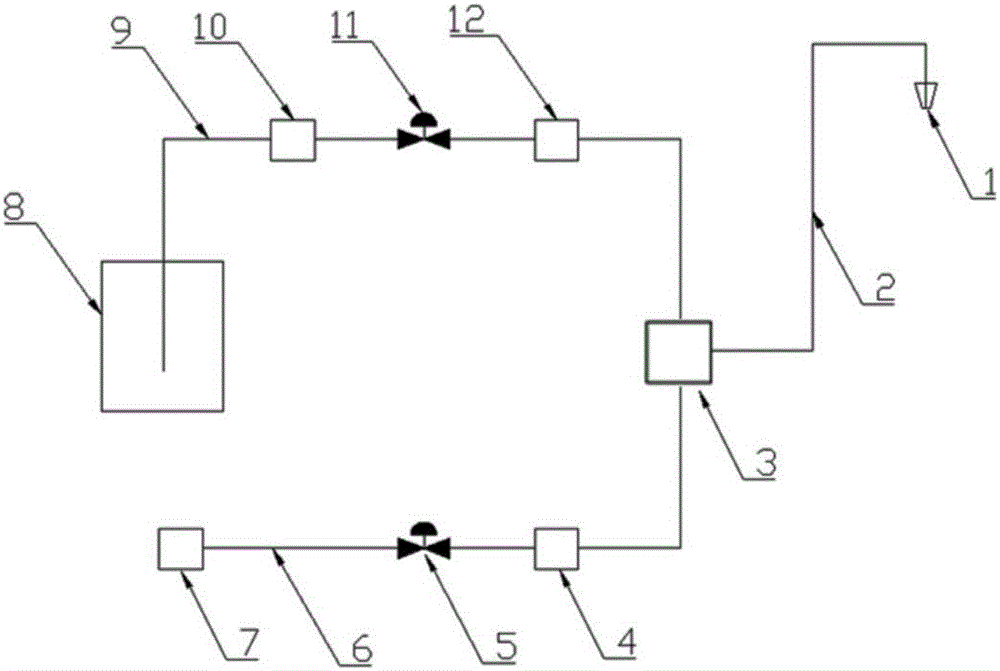
[0041] In the following specific embodiments of the present invention, please refer to figure 1 , figure 1 It is a structural schematic diagram of a wafer cleaning device in a preferred embodiment of the present invention. The wafer cleaning device of the present invention can be used to clean the wafers placed on the rotating platform in the clean...


PUM


Abstract

The invention discloses a wafer cleaning device and a cleaning method. The cleaning device includes a cleaning medium spray part and a cleaning medium control part. The cleaning medium spray part includes a nozzle, a movable spray pipeline connected to the nozzle, and a cleaning medium control part. It includes first and second pipelines connected in parallel with a mixing chamber, and the mixing chamber is connected to the spray pipeline; wherein, the first pipeline has a Venturi tube structure at its interface with the mixing chamber, and the first pipeline The liquefied first gas fed through the first pipeline is ejected to the mixing chamber through the Venturi tube structure, forming a three-phase state in which solid, liquid and gas coexist, and is jointly formed by the second gas fed through the second pipeline. The cleaning medium is sprayed onto the surface of the wafer to be cleaned through the nozzle along the spraying pipeline, which can realize physical cleaning of the wafer without damage, simplify the cleaning process, and reduce production costs at the same time.

Description

technical field [0001] The present invention relates to the technical field of semiconductor cleaning equipment, and more specifically, to a wafer cleaning device and a cleaning method thereof that can simultaneously provide solid, liquid, and gas three-phase cleaning media to clean wafers without damage. Background technique [0002] The cleaning process is the most common process step in the integrated circuit manufacturing process, and its purpose is to effectively control the pollution level of each process step to achieve the goal of each process step. [0003] In order to remove the contamination on the surface of the wafer, when performing, for example, a single-wafer wet cleaning process, the wafer will be placed on the rotating platform (such as a spin chuck) of the cleaning equipment and rotated at a certain speed; The surface of the circle is sprayed with a certain flow rate of cleaning liquid to clean the surface of the wafer. [0004] While achieving the purpos...

Claims


Application Information

Patent Timeline
IPC IPC(8): H01L21/67H01L21/02
CPCH01L21/67017H01L21/02057H01L21/02082
Inventor 滕宇
Owner BEIJING SEVENSTAR ELECTRONICS CO LTD
Why Eureka
Try Eureka