A cob light source light output structure and its application

A light source and grid technology, which is applied in the field of COB light source light structure, can solve the problems of low luminous efficiency and uniformity of chips, low luminous efficiency and uniformity of light sources, and increased relative quantity of reflected light, etc., to achieve good color temperature consistency of light sources, Increased luminous flux and low heat generation

Active Publication Date: 2018-04-03
临清芯圆半导体有限公司
View PDF6 Cites 0 Cited by
  • Summary
  • Abstract
  • Description
  • Claims
  • Application Information

AI Technical Summary

Problems solved by technology

[0002] The conventional COB light source structure will cause multiple total reflections of light inside the light source, resulting in increased heat generation, reduced luminous efficiency, and low light uniformity. Especially for high-power COB light sources, the chip density is higher than that of a single SMD light source. more pronounced reduction
like figure 1 Shown is the light path diagram of the total reflection of the conventional COB light source structure. The total reflection of light 2 causes multiple total emission of light 2 on the interface between the filled silica gel and the air. and uniformity are low
like figure 2 Shown is a schematic structural diagram of a conventional COB light source structure, image 3 for figure 2 In the enlarged picture of part B, the conventional COB light source has a simple structure, no light output structure, total reflection cannot be reduced, and the luminous efficiency and uniformity of the light source are low
[0003] In addition, the density of the chip in the conventional COB light source structure should not be too large. If the density is too high, the relative area of ​​the chip on the heat dissipation substrate will increase, and the relative amount of reflected light absorbed by the surface of the chip will increase, resulting in low overall light extraction efficiency.

Method used


Image

  • A cob light source light output structure and its application
  • A cob light source light output structure and its application
  • A cob light source light output structure and its application

Examples


Embodiment Construction

[0021] The present invention will be further described below in conjunction with the accompanying drawings.

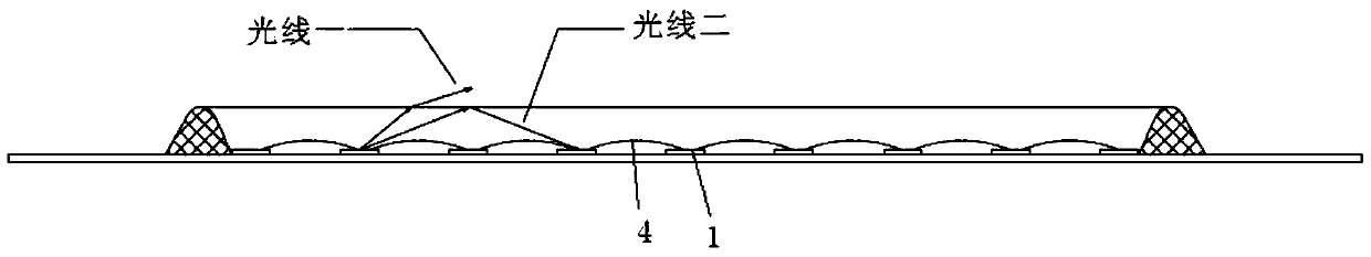
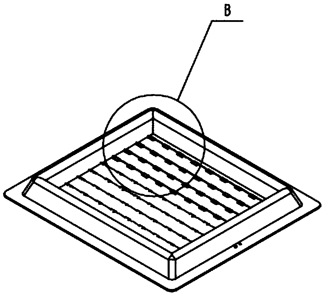
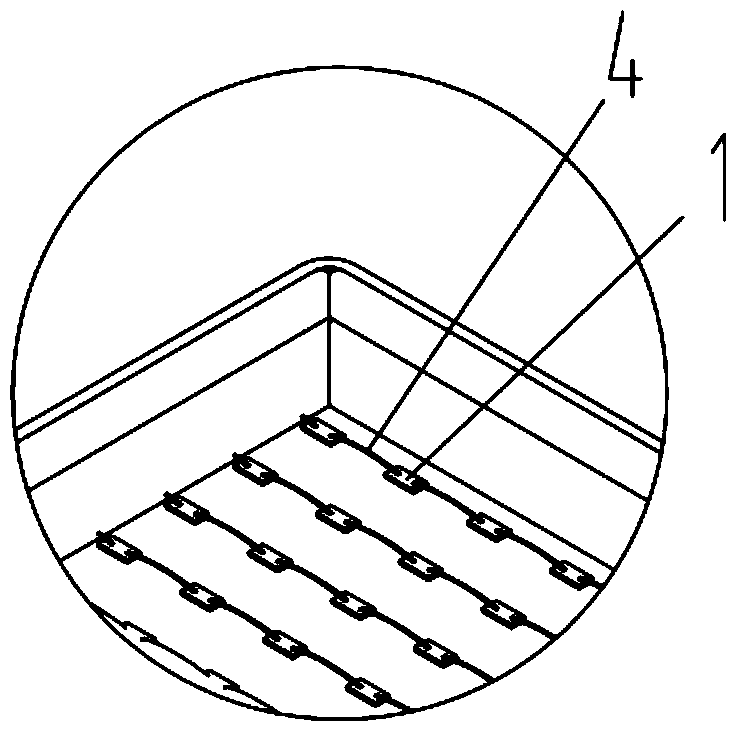
[0022] like Figure 1~Figure 7 As shown in the figure, a light-emitting structure of a COB light source is characterized in that it includes: a grid 2 separating adjacent wafers 1, the grid 2 includes grid bars 3 with a triangular cross-section in a crisscross pattern. The bottom end of the grid bars 3 is provided with a number of notches 5 for passing through the bonding wires 4 .

[0023] The notch 5 includes a V-shaped notch.

[0024] The material of the grille 2 includes white PC or white silica gel.

[0025] The height of the grid 2 is the same as the height of the filled silica gel.

[0026] The grille 2 is arranged on the heat dissipation substrate, and the cup-shaped cavities enclosed by the grille 2 and the heat dissipation substrate are filled with the filled silica gel; the bottom surface area of ​​the cup-shaped cavity is smaller than the top surface. a...


PUM


Abstract

The invention discloses a light output structure of a COB light source, which is characterized in that it comprises: a grid (2) separating adjacent wafers (1), and the grid (2) includes criss-crossing cross-sections that are triangular The grid bar (3), the bottom end of the grid bar (3) is provided with several notches (5) for passing through the welding wire (4). The invention also discloses the application of a COB light source light output structure, which is characterized in that: the grid (2) is applied to COB light source products of various wattages. The light output structure of a COB light source and its application provided by the present invention solve the problem of low light output efficiency caused by the high chip density of the lighting COB light source in the prior art, and solve the problem of mutual absorption of light between chips when used, and have a structure Simple, low cost, high luminous efficiency, and good color temperature consistency of the light source, it is a very simple and practical COB light source structure.

Description

technical field [0001] The invention relates to a light emitting structure of a COB light source and its application, in particular to an integrated light emitting structure and its application which can effectively improve the luminous efficiency and uniformity of the light source. Background technique [0002] The conventional COB light source structure will lead to multiple total reflections of light inside the light source, resulting in increased light source heating, reduced luminous efficiency, and low light uniformity, especially for high-power COB light sources. decrease is more pronounced. like figure 1 Shown is the optical path diagram of the total reflection of the conventional COB light source structure. The total reflection of light 2 results in multiple total emission of light 2 at the interface between the filled silica gel and the air. Light 2 is not easy to exit the interface, resulting in the luminous efficiency of the chip. and uniformity are low. like ...

Claims


Application Information

Patent Timeline
Patent Type & Authority Patents(China)
IPC IPC(8): H01L25/13H01L33/48H01L33/60
CPCH01L2224/48091H01L2224/48137H01L2924/00014
Inventor 洪春旭王钢
Owner 临清芯圆半导体有限公司
Why Eureka
Try Eureka