Roughened flip-chip GAAS-based LED epitaxial wafer grown on a SIC or SI pattern substrate and preparation method thereof
An LED epitaxial wafer and substrate technology, applied in the field of optoelectronics, can solve the problem of no introduction, etc., and achieve the effects of improving the light extraction rate, increasing the roughening area, and reducing the harm
- Summary
- Abstract
- Description
- Claims
- Application Information
AI Technical Summary
Problems solved by technology
Method used
Image
Examples
Embodiment 1
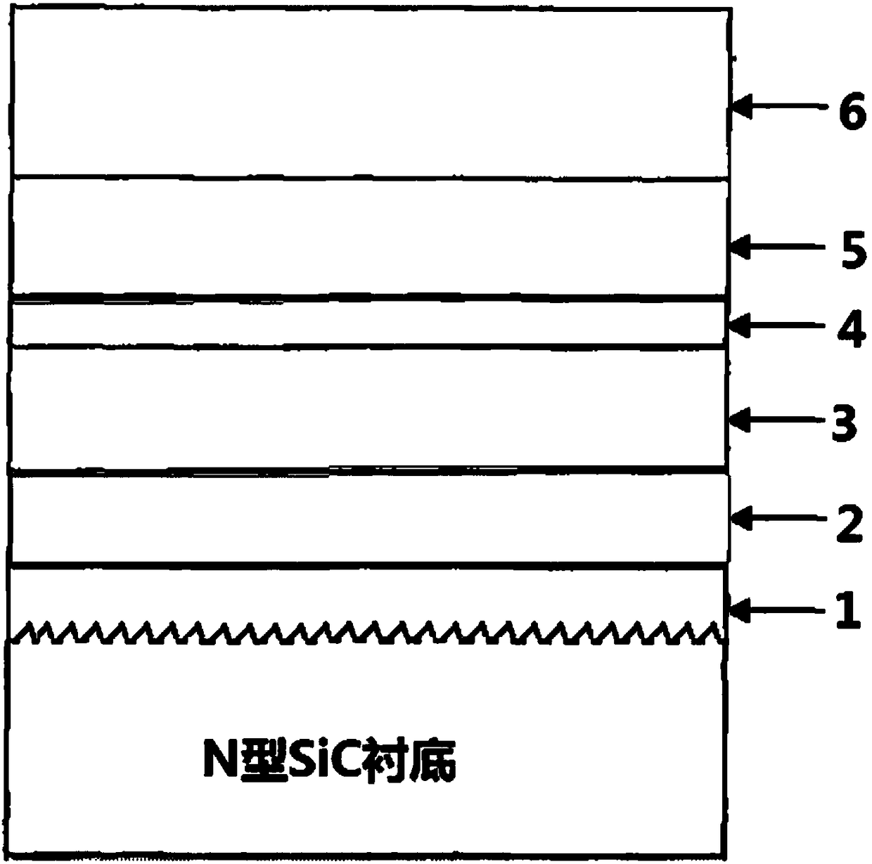
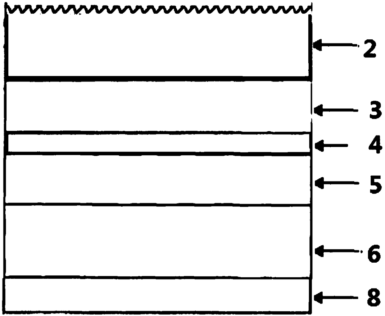
[0063] An N-type SiC pattern substrate flip-chip LED epitaxial wafer, such as image 3 As shown, it includes a corrosion barrier layer 2, an AlInP lower confinement layer 3, a multi-quantum well light-emitting region 4, an AlInP upper confinement layer 5, a current spreading layer 6, and a SiC substrate 8 from top to bottom, and the corrosion barrier layer 2 is provided with cylinder.
[0064] The setting of the cylinder increases the roughness of the surface, improves the light extraction efficiency of the flip-chip GaAs-based LED epitaxial wafer, and makes the actual light extraction rate reach more than 90%, which solves the problem of low light extraction efficiency.
[0065] The corrosion barrier layer 2 is periodically provided with cylinders, the period of the cylinders is 500nm, the depth of the depressions of the cylinders is 3um, and the height of the protrusions of the cylinders is 50um.
Embodiment 2
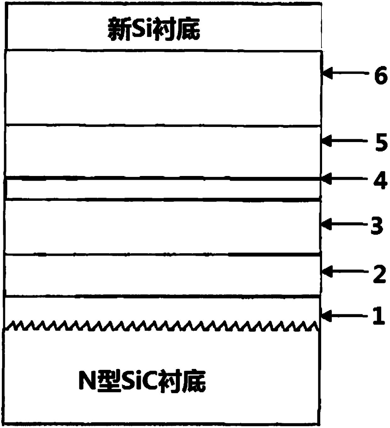
[0067] A method for growing the flip-chip LED epitaxial wafer described in Embodiment 1 on an N-type SiC pattern substrate, the specific steps comprising:
[0068] (1) Using a dry etching method, etch on the surface of the original N-type SiC substrate to make an N-type SiC pattern substrate; specifically include:
[0069] (I) Evaporate SiO with a thickness of 800 angstroms on the pristine N-type SiC substrate 2 ;
[0070] (Ⅱ) on SiO 2 Apply photoresist evenly on the surface, and cover with different pre-engraved pattern masks; the pattern masks are circular;
[0071] (Ⅲ) Expose the area other than the area covered by the pattern mask, and use a photolithography machine to carve out the mask pattern;
[0072] (IV) Develop in NaOH solution for 35 seconds to expose SiO with mask pattern 2 , the mass concentration of NaOH solution is 3%, and it is etched with HF acid for 1 minute, and the acid etches away SiO 2 , exposing the N-type SiC substrate;
[0073] (Ⅴ) Etch the phot...
Embodiment 3
[0091] A flip-chip LED epitaxial wafer with a P-type SiC pattern substrate, which sequentially includes a corrosion barrier layer 2, an AlInP lower confinement layer 3, a multi-quantum well light-emitting region 4, an AlInP upper confinement layer 5, a current spreading layer 6, and SiC from top to bottom. The substrate 8 and the corrosion barrier layer 2 are provided with rhomboids.
[0092] The arrangement of rhomboids increases the roughness of the surface, improves the light extraction efficiency of the flip-chip GaAs-based LED epitaxial wafer, makes the actual light extraction rate reach more than 90%, and solves the problem of low light extraction efficiency.
[0093] The corrosion barrier layer 2 is periodically provided with rhomboids, the period of the rhomboids is 500nm, the depth of the rhombus concave is 3um, and the height of the rhombus protrusion is 50um.
PUM
| Property | Measurement | Unit |
|---|---|---|
| height | aaaaa | aaaaa |
| thickness | aaaaa | aaaaa |
| thickness | aaaaa | aaaaa |
Abstract
Description
Claims
Application Information
 - R&D
- Intellectual Property
- Life Sciences
- Materials
- Tech Scout
- Unparalleled Data Quality
- Higher Quality Content
- 60% Fewer Hallucinations
Browse by: Latest US Patents, China's latest patents, Technical Efficacy Thesaurus, Application Domain, Technology Topic, Popular Technical Reports.
© 2025 PatSnap. All rights reserved.Legal|Privacy policy|Modern Slavery Act Transparency Statement|Sitemap|About US| Contact US: help@patsnap.com


