Display substrate, manufacturing method thereof, and display device

A technology for display substrates and display devices, applied in identification devices, semiconductor/solid-state device manufacturing, instruments, etc., can solve the problems of low light output efficiency of display substrates, low light output efficiency of display devices, improve light output efficiency, avoid total reflection, and solve light output problems. less efficient effect

Active Publication Date: 2018-06-05
BOE TECH GRP CO LTD +1
View PDF4 Cites 0 Cited by
  • Summary
  • Abstract
  • Description
  • Claims
  • Application Information

AI Technical Summary

Problems solved by technology

[0005] In order to solve the problem of low light extraction efficiency of the display substrate and the low light extraction efficiency of the display device, the present invention provides a display substrate, a manufacturing method thereof, and a display device

Method used


Image

  • Display substrate, manufacturing method thereof, and display device
  • Display substrate, manufacturing method thereof, and display device
  • Display substrate, manufacturing method thereof, and display device

Examples


Embodiment Construction

[0055] In order to make the object, technical solution and advantages of the present invention clearer, the present invention will be further described in detail below in conjunction with the accompanying drawings. Obviously, the described embodiments are only some embodiments of the present invention, rather than all embodiments . Based on the embodiments of the present invention, all other embodiments obtained by persons of ordinary skill in the art without making creative efforts belong to the protection scope of the present invention.

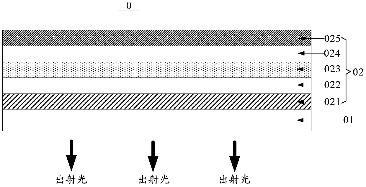
[0056] Please refer to figure 1 , which shows a schematic structural diagram of a display substrate 0 provided by an embodiment of the present invention, see figure 1 , the display substrate 0 may include a base substrate 01, and the base substrate 01 may be a transparent substrate, specifically, a substrate made of light-guiding and non-metallic materials with certain firmness such as glass, quartz, and transparent resin.

[0057] The ba...


PUM


Abstract

The invention discloses a display substrate, a manufacturing method thereof, and a display device, belonging to the technical field of display. The display substrate includes: a base substrate, on which a first light-emitting unit is arranged, and the first light-emitting unit includes: a first selective reflective transmission layer, an anode layer, a first organic light-emitting layer, a cathode layer and a reflective layer stacked in sequence ; Wherein, the first organic light-emitting layer can emit colored light under the action of the anode layer and the cathode layer, and the first selective reflective transmission layer and the reflective layer can reflect the colored light, so that the colored light can be reflected in the first selective Vibration between the reflective transmissive layer and the reflective layer, through the first selective reflective transmissive layer emitted from the base substrate, the present invention solves the problem of low light extraction efficiency of the display substrate and the display device, and improves the efficiency of the display substrate and the display device The effect of light efficiency. The invention is used for display.

Description

technical field [0001] The invention relates to the field of display technology, in particular to a display substrate, a manufacturing method thereof, and a display device. Background technique [0002] An organic light-emitting diode (English: Organic Light-Emitting Diode; abbreviation: OLED) display device is a display device with an autonomous light emitting function. Because it does not require a backlight, and has the advantages of high contrast, thin thickness, wide viewing angle, fast response, high and low temperature resistance, etc., it has broad prospects in the display industry. [0003] OLED display devices can generally include a display substrate. In the prior art, the display substrate includes a base substrate, and three light-emitting units stacked in sequence are arranged on the base substrate. For example, the three light-emitting units include: a red light unit, Green light unit and blue light unit, each light-emitting unit includes: a cathode layer, an...

Claims


Application Information

Patent Timeline
Patent Type & Authority Patents(China)
IPC IPC(8): H01L21/77H01L27/12H01L27/32G09F9/33
CPCG09F9/33H01L21/77H01L27/12H10K59/00H10K85/6565H10K85/654H10K50/856H10K50/19H10K50/13H10K71/00H10K85/60H10K85/624H10K85/626H10K85/653H10K85/6572H10K85/6574
Inventor 杨钰婷叶纯李琨章善财
Owner BOE TECH GRP CO LTD
Why Eureka
Try Eureka