

Power semiconductor device
a semiconductor device and power semiconductor technology, applied in semiconductor devices, transistors, electrical devices, etc., can solve the problems of increasing the turn-off time, the delay of the depletion layer from the start of the voltage rise, and the large noise of the switching, so as to improve the injection efficiency of carriers and increase the resistance against flow
- Summary
- Abstract
- Description
- Claims
- Application Information
AI Technical Summary
Benefits of technology
Problems solved by technology
Method used
Image

Examples
first embodiment
[0129](First Embodiment)
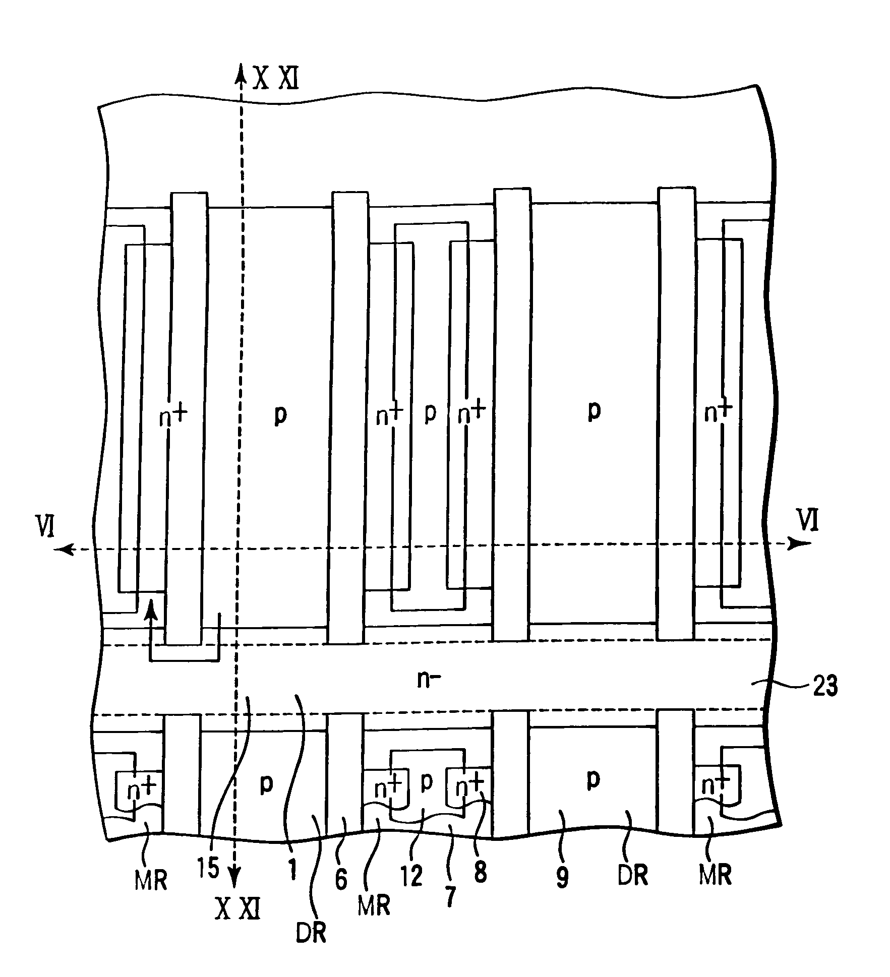
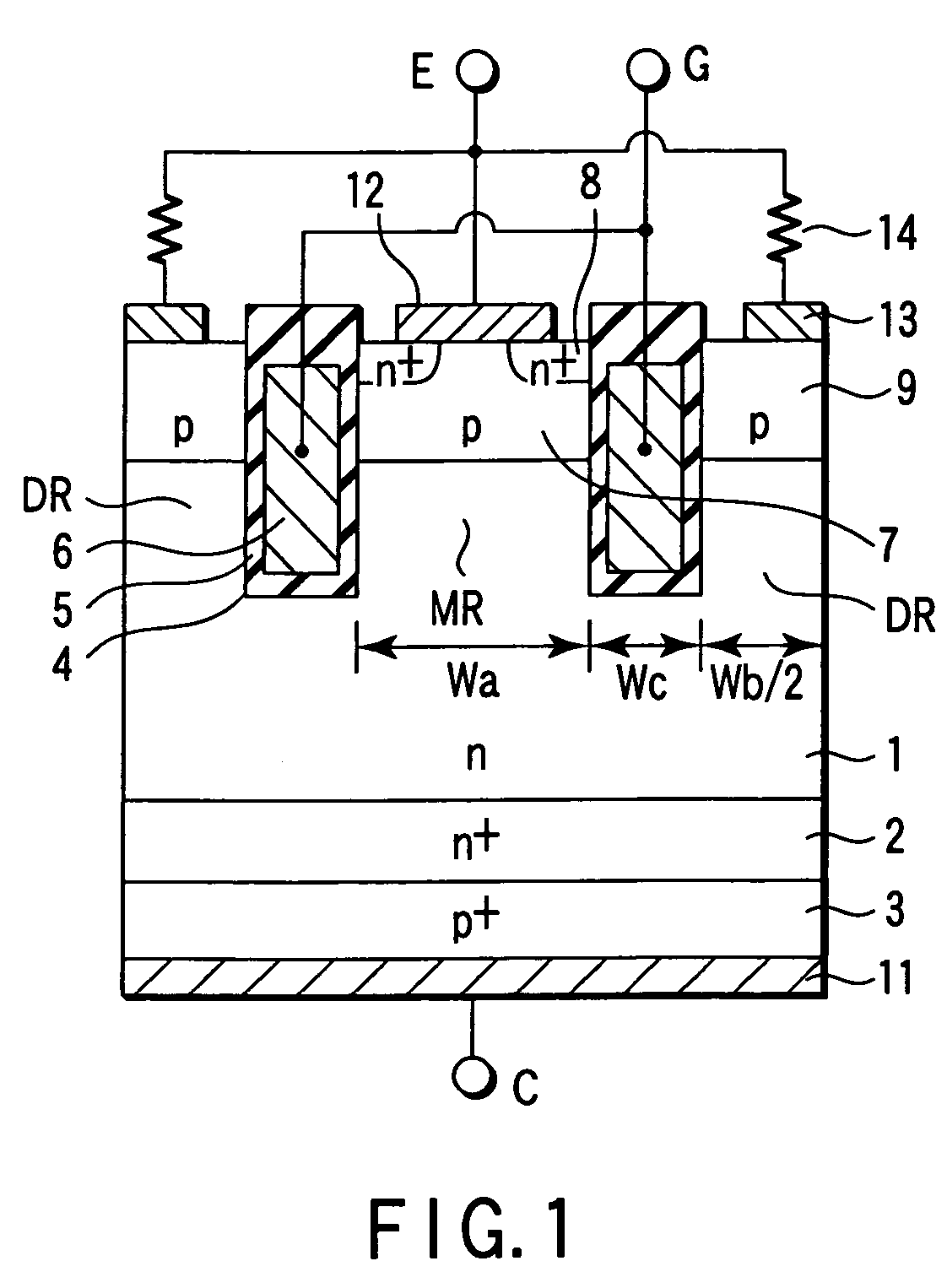
[0130]FIG. 1 is a sectional view showing a power semiconductor device (IEGT) according to a first embodiment of the present invention. As shown in FIG. 1, on one side of an n-base layer 1 having a high resistivity, an n-buffer layer 2 having a high impurity concentration is disposed, and a p-collector layer 3 having a high impurity concentration is further disposed thereon. The n-buffer layer 2 may be omitted such that the p-collector layer 3 is in direct contact with the n-base layer 1. On the other side of the n-base layer 1, a plurality of trenches 4 are formed at intervals in the n-base layer 1, such that main cells MR and dummy cells DR are partitioned.
[0131]In each of the main cells MR, a p-base layer 7 is disposed on the n-base layer 1. N-emitter layers 8 are formed in the surface of the p-base layer 7. In each of the dummy cells DR, a p-buffer layer 9 is disposed on the n-base layer 1. The p-base layers 7 and p-buffer layers 9 may be formed independen...
second embodiment
[0153](Second Embodiment)
[0154]FIG. 5 is a view showing the plan layout of a power semiconductor device (IEGT) according to a second embodiment of the present invention. FIG. 6 is a sectional view taken along line VI—VI in FIG. 5. This embodiment adopts a buffer resistor 14 mainly employing a lateral resistance of a p-buffer layer 9. In other words, the buffer resistor 14 is planarly structured.
[0155]Specifically, the surface of the p-buffer layer 9 in each of dummy cells DR is covered with an insulating film 10. However, a buffer electrode 13 electrically connected to an emitter electrode 12 is disposed on that portion of the p-buffer layer 9, which corresponds to a position beyond the end of n-emitter layers 8 in the channel width direction. Accordingly, the buffer resistor 14 includes a lateral resistance of the p-buffer layer 9 as a main component, on the route from that portion of the p-buffer layer 9, which faces the n-emitter layers 8, to the buffer electrode 13.
[0156]The buf...
third embodiment
[0157](Third Embodiment)
[0158]FIG. 7 is a view showing the plan layout of a power semiconductor device (IEGT) according to a third embodiment of the present invention. The sectional view taken along line VI—VI in FIG. 7 is the same as that shown in FIG. 6. This embodiment also adopts a buffer resistor 14 mainly employing a lateral resistance of a p-buffer layer 9.
[0159]Specifically, each of trenches 4 including a gate electrode 6 is cut at predetermined intervals, while an emitter electrode 12 is continuously formed on each of main cells MR including the cut portion of the trench 4. The p-buffer layer 9 is electrically connected to the emitter electrode 12 through a p-connection layer 16 present at the cut portion of the trench 4. Accordingly, the buffer resistor 14 includes a lateral resistance of the p-buffer layer 9 as a main component, on the route from that portion of the p-buffer layer 9, which faces n-emitter layers 8, to the emitter electrode 12 through the p-connection laye...
PUM
 Abstract
Description
Claims
Application Information