Atomic composition controlled ruthenium alloy film formed by plasma-enhanced atomic layer deposition

a technology of atomic composition control and ruthenium alloy, which is applied in the direction of synthetic resin layered products, natural mineral layered products, and semiconductor/solid-state device details, etc., can solve the problems of loss of reliability of wiring, high film resistivity, via resistance, etc., and achieves the effect of increasing flow rate ratio, reducing density, and increasing resistan

Active Publication Date: 2011-12-27
ASM JAPAN
View PDF272 Cites 330 Cited by
  • Summary
  • Abstract
  • Description
  • Claims
  • Application Information

AI Technical Summary

Benefits of technology

[0015]In view of the above, the inventors examined combinations of Ta material and Ru material. In particular, the inventors examined materials that can be broken down by H2 plasma or H2 / N2 plasma. Furthermore, the inventors examined an optimal composition in the depth direction of a film made by these materials, and a method for controlling such composition, in order to ensure adhesion and barrier property of the film as a Cu wiring liner. In an embodiment of a method for forming a RuTaN film being a Cu barrier film, combining Ta material with H2 / N2 plasma, and Ru material with H2 / N2 plasma, is effective. A stable RuTaN film can be formed by increasing the flow rate ratio of N2 or adjusting the H2 / N2 plasma time. If H2 plasma is applied after the supply of Ta material, the residual carbon content in the film increases, thereby resulting in lower density and higher resistance. When H2 / N2 plasma is applied, on the other hand, the resistance becomes lower and the residual carbon content decreases. Accordingly, it is effective to use plasma of H2 / N2 mixed gas after the supply of Ta material. In the meantime, in an embodiment a RuTa film containing less N can be formed by combining Ta material with H2 / N2 plasma, and Ru material with H2 plasma. In this case, the resistivity can be lowered by reducing the N content, and also stable resistivity can be achieved according to the H2 plasma conditions. To be specific, the residual carbon content drops due to H2 / N2 gas plasma applied after the supply of Ta material, and the nitrogen content can also be reduced by hydrogen plasma applied after the supply of Ru material, which allows for formation of a RuTa alloy offering lower resistance.
[0016]The aforementioned method is effective when specific Ta and Ru materials are used. Particularly with the Ru material, use of a material that can easily be broken down by H2 plasma is effective in controlling the N content. This is not possible with conventional Ru(EtCp)2. An example of such effective material is one coordinated by two β-diketone groups. Accordingly, in an embodiment an optimal liner film in terms of adhesion, Cu barrier property and resistivity can be formed by plasma atomic layer deposition in a single process that can be carried out continuously in the same reaction apparatus, by using these effective materials along with the aforementioned plasma step and by also controlling the composition of the film in the depth direction in a manner appropriate for a Cu wiring liner film. In other words, the adhesion with the Cu wiring in the bottom layer, adhesion with the Cu wiring in the top layer, and Cu diffusion barrier property can be further optimized by controlling the composition of Ru, Ta and N in the depth direction.
[0018]By utilizing inventions 1), 2) and 3) mentioned above, a Cu barrier metal film constituted by RuTa can be provided, wherein such film maintains adhesion, Cu barrier property and low resistivity in next-generation, fine, highly integrated Cu wiring structures having high aspect ratios, and has its composition controlled in the depth direction through plasma atomic layer deposition to ensure excellent coverage.

Problems solved by technology

However, the prior arts mentioned above are associated with at least the problems explained below.
However, use of NH3 plasma or H2 / N2 plasma promotes nitriding of the Ta layer formed as the bottom layer, resulting in significantly high film resistivity.
Accordingly, applying the present invention to via holes connecting the top-layer Cu wiring layer and bottom-layer Cu wiring, which is the object of the aforementioned published example, will significant increase the via resistance and result in loss of reliability of wiring.
In addition, the amount of Ru needs to be increased to lower the wiring resistance, and therefore the adhesion with the insulation film tends to drop as the amount of Ru increases.
These differences make it difficult to achieve good adhesion at the top and bottom interfaces based on the same film quality.
Korean Patent Application No. 10-2005-0103373 also presents a problem of increased resistivity due to nitriding of Ta by NH3 plasma.
As is the case with the aforementioned paper by C. C. Yong et al., it is difficult to achieve good wiring reliability relative to both the top layer and bottom layer using only an alloy having a specific composition of amorphous Ta and Ru, because Ru provides good adhesion with copper in the top layer, while TaN provides good adhesion with the inter-layer insulation film in the bottom layer.

Method used


Image

  • Atomic composition controlled ruthenium alloy film formed by plasma-enhanced atomic layer deposition
  • Atomic composition controlled ruthenium alloy film formed by plasma-enhanced atomic layer deposition
  • Atomic composition controlled ruthenium alloy film formed by plasma-enhanced atomic layer deposition

Examples


example 1

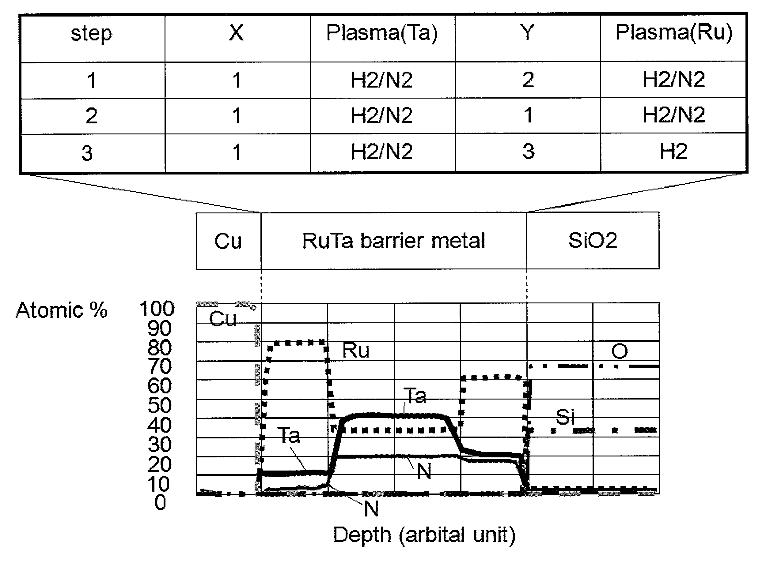
[0146]A specific example where the process in FIG. 1 is implemented using the apparatus shown in FIG. 4 based on the process sequences shown in FIGS. 5 and 6 is explained.

[0147]A Cu wiring is formed according to the process shown in FIG. 7 in a Cu wiring forming process based on dual damascene structure. Silicon substrates having a device that has been processed up to the state in FIG. 7(a) are treated using the apparatus shown in FIG. 10. A silicon substrate is set in a cassette loader 501, and a transfer robot 502 is used to transfer the substrate into a load lock chamber 503, after which the substrate is transferred by a vacuum robot 504 from the load lock chamber 503 into a reaction chamber for plasma atomic layer deposition 505. The next substrate is transferred to a reaction chamber 507, and the subsequent substrate is transferred to a reaction chamber 508, to allow the process to be implemented in a similar manner. The substrate transferred to the reaction chamber 505 is plac...

example 2

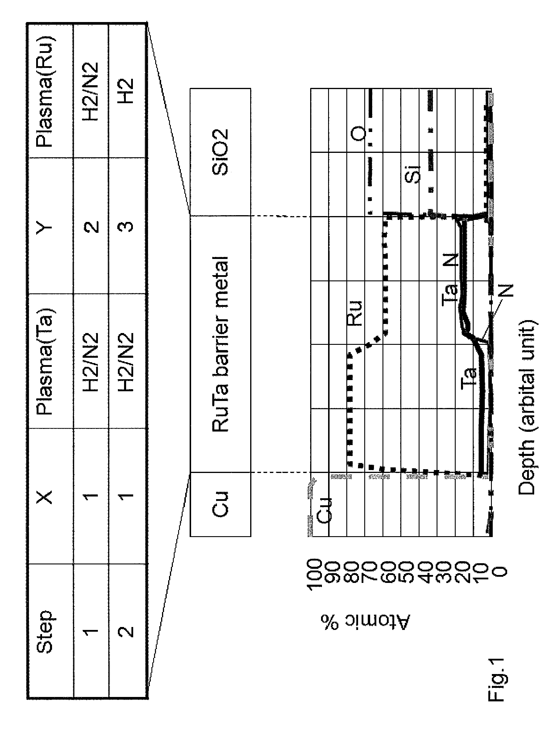
[0153]A specific example where the process in FIG. 2 is implemented using the apparatus shown in FIG. 4 based on the process sequences shown in FIGS. 5 and 6 is explained.

[0154]A Cu wiring is formed according to the process shown in FIG. 8 in a Cu wiring forming process based on dual damascene structure. Silicon substrates having a device that has been processed up to the state in FIG. 8(a) are treated using the apparatus shown in FIG. 10. A silicon substrate is set in a cassette loader 501, and a transfer robot 502 is used to transfer the substrate into a load lock chamber 503, after which the substrate is transferred by a vacuum robot 504 from the load lock chamber 503 into a reaction chamber for plasma atomic layer deposition 505. The next substrate is transferred to a reaction chamber 507, and the subsequent substrate is transferred to a reaction chamber 508, to allow the process to be implemented in a similar manner. The substrate transferred to the reaction chamber 505 is plac...

example 3

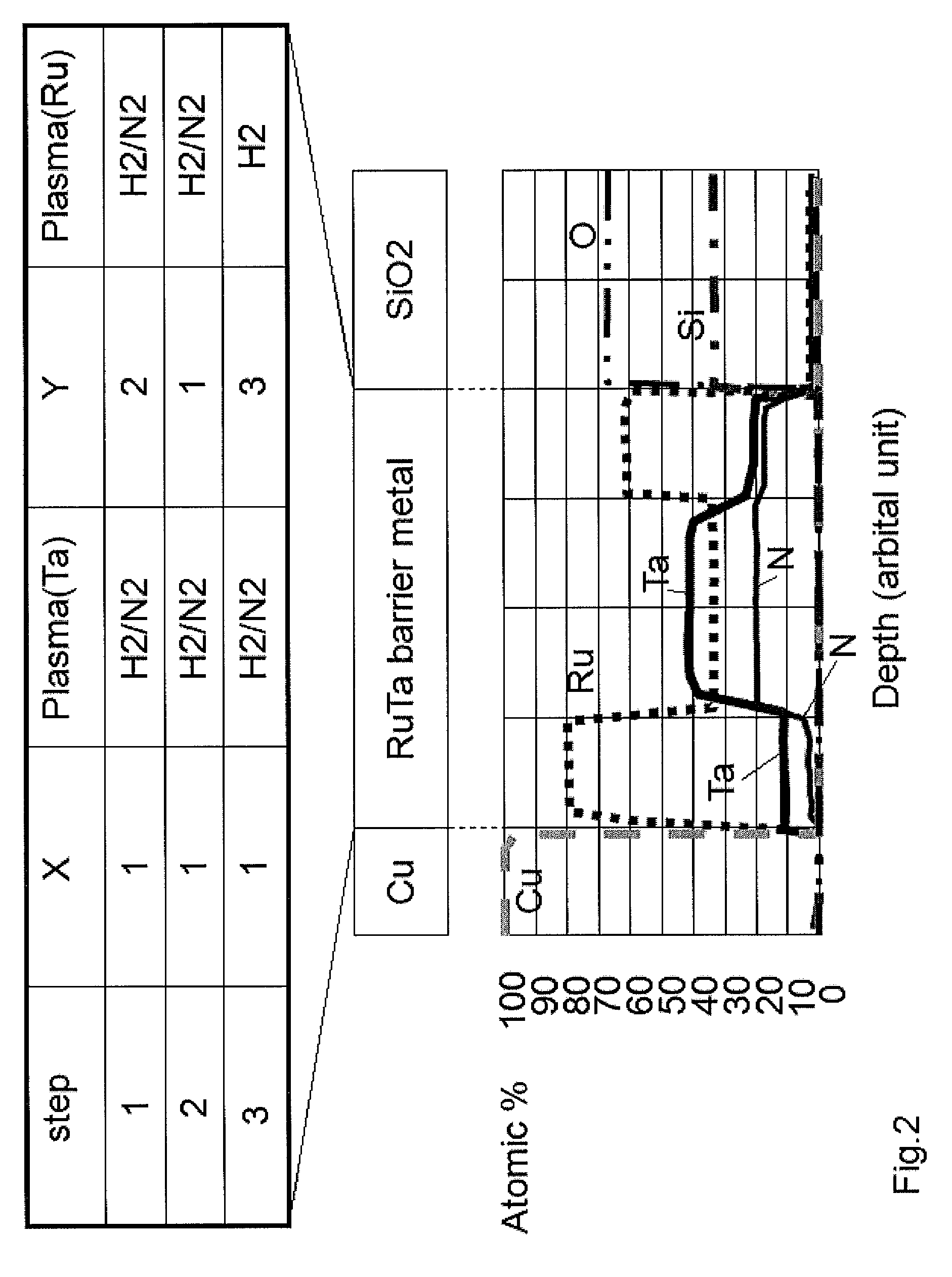
[0157]A specific example where the process in FIG. 1 is implemented using the apparatus shown in FIG. 4 based on the process sequences shown in FIGS. 5 and 6 is explained.

[0158]A Cu wiring is formed according to the process shown in FIG. 9 in a Cu wiring forming process based on dual damascene structure. Silicon substrates having a device that has been processed up to the state in FIG. 9(a) are treated using the apparatus shown in FIG. 10. A silicon substrate is set in a cassette loader 501, and a transfer robot 502 is used to transfer the substrate into a load lock chamber 503, after which the substrate is transferred by a vacuum robot 504 from the load lock chamber 503 into a reaction chamber for plasma atomic layer deposition 505. The next substrate is transferred to a reaction chamber 507, and the subsequent substrate is transferred to a reaction chamber 508, to allow the process to be implemented in a similar manner. The substrate transferred to the reaction chamber 505 is plac...


PUM

PropertyMeasurementUnit
thicknessaaaaaaaaaa
thicknessaaaaaaaaaa
total thicknessaaaaaaaaaa

Abstract

A metal film composed of multiple atomic layers continuously formed by atomic layer deposition of Ru and Ta or Ti includes at least a top section and a bottom section, wherein an atomic composition of Ru, Ta or Ti, and N varies in a thickness direction of the metal film. The atomic composition of Ru, Ta or Ti, and N in the top section is represented as Ru(x1)Ta / Ti(y1)N(z1) wherein an atomic ratio of Ru(x1) / (Ta / Ti(y1)) is no less than 15, and z1 is 0.05 or less. The atomic composition of Ru, Ta or Ti, and N in the bottom section is represented as Ru(x2)Ta / Ti(y2)N(z2) wherein an atomic ratio of Ru(x2) / (Ta / Ti(y2)) is more than zero but less than 15, and z2 is 0.10 or greater.

Description

BACKGROUND[0001]1. Field of the Invention[0002]The present invention relates to a method for forming a Cu diffusion barrier metal for metal wiring structures that can be favorably used in the creation of fine semiconductor elements in general, as well as a structure of such Cu diffusion barrier metal.[0003]2. Description of the Related Art[0004]Ru film is drawing the attention for its property to improve the adhesion with Cu, when a Ru film is formed at the interface between Cu and barrier metal in a Cu wiring structure which is the main wiring structure used in high-speed logic elements such as MPUs, and thereby significantly enhance the reliability of wiring. Methods are being studied to form a Ru film that provides a Cu wiring liner on a TaN film or WN film and then form a Cu film on top of the Ru film (one example of such method relating to a combination of Ru and TaN is described in C. C. Yong et al., “Physical, Electrical, and Reliability Characterization of Ru for Cu Intercon...

Claims


Application Information

Patent Timeline
Patent Type & Authority Patents(United States)
IPC IPC(8): C23C16/00
CPCC23C16/34C23C16/4554H01L21/28562H01L21/76846H01L23/53238H01L2924/0002H01L2924/00
Inventor SHINRIKI, HIROSHINAMBA, KUNITOSHIJEONG, DAEKYUN
Owner ASM JAPAN
Why Eureka
Try Eureka