

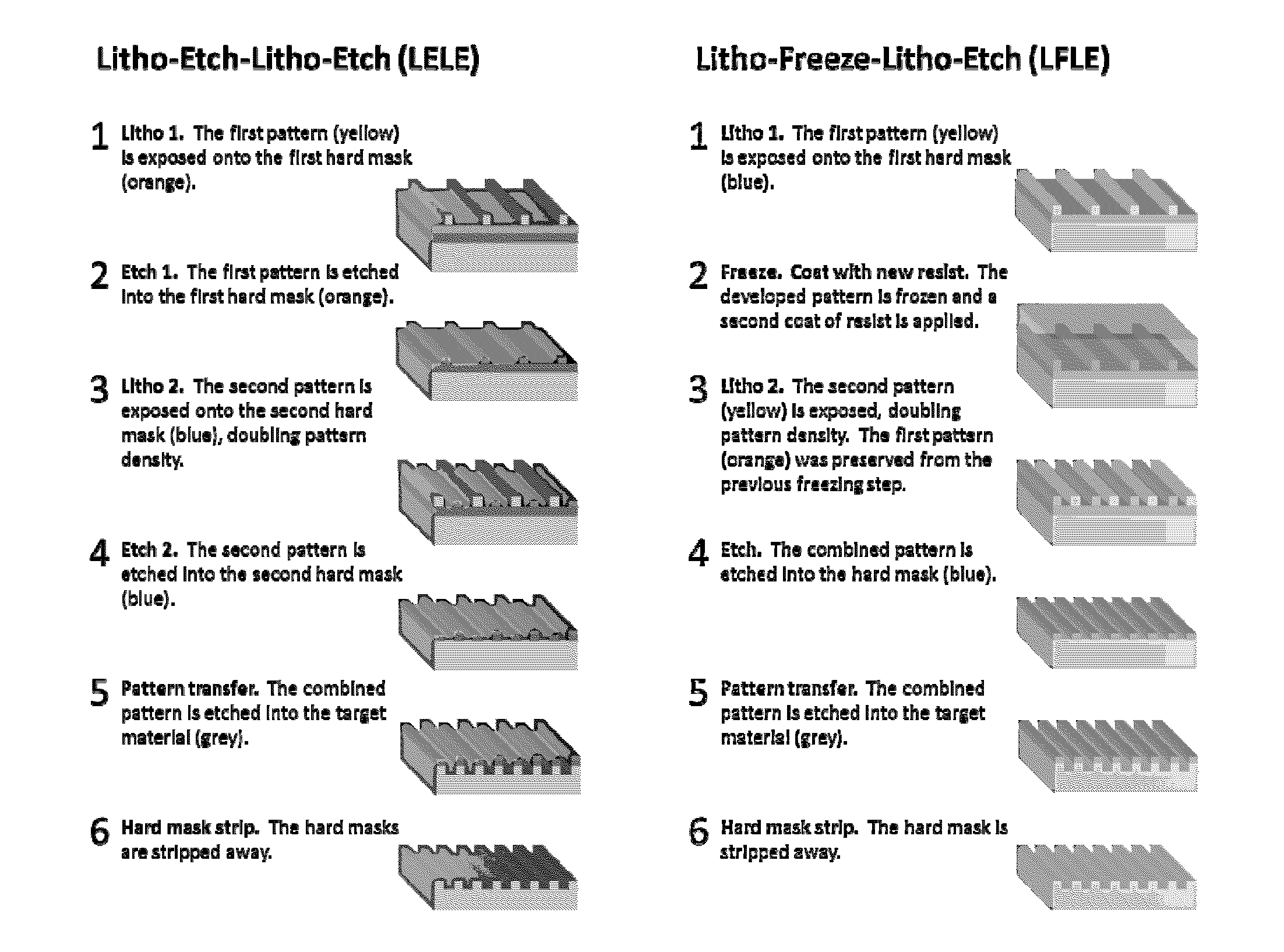
Sequential Infiltration Synthesis for Enhancing Multiple-Patterning Lithography
a lithography and multiple-pattern technology, applied in the field of photolithography, can solve the problems of reducing reducing the quality of lithography, so as to increase the plasma etch resistance, reduce the number of steps, and improve the effect of lithography quality
- Summary
- Abstract
- Description
- Claims
- Application Information
AI Technical Summary
Benefits of technology
Problems solved by technology
Method used
Image

Examples
examples
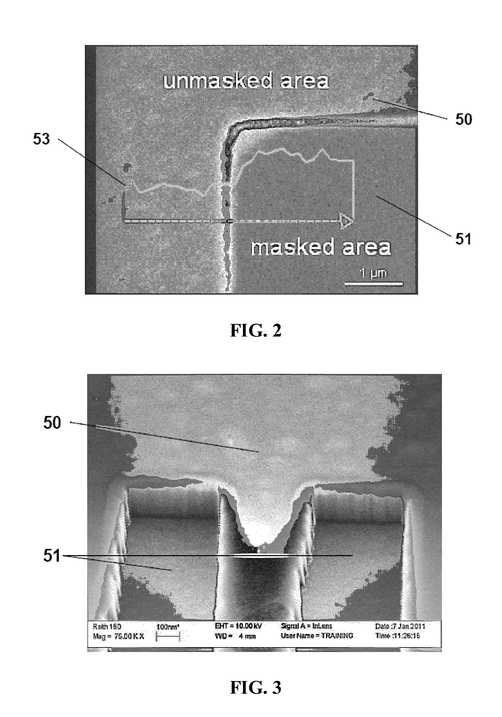
[0047]In order to demonstrate the properties of a substrate modified with SIS prior to lithography, an SIS-patterned PMMA resist layer was created.
[0048]With reference to FIGS. 4A-4D and FIG. 5, the PMMA resist layer 201 is applied (step 101) to a substrate 202 such as a silicon substrate. In various embodiments, spin coating may be used to apply the resist layer 201 to the substrate 202; however, other techniques may also be used. Next, a pattern 203 (shown in FIG. 4B) may be applied to the resist layer (step 102). Patterning of the resist layer 201 may be accomplished by a variety of processes known in the art including electron beam exposure, photolithography and polymer self-assembly processes such as block copolymer. In various embodiments, selected areas of the PMMA resist layer are exposed to an electron beam or photons to form the pattern 203. The resist layer 201 is then developed (step 103) using chemical developers such as methyl isobutyl ketone and isopropyl alcohol (MIB...
PUM
| Property | Measurement | Unit |
|---|---|---|
| wavelength | aaaaa | aaaaa |
| wavelength | aaaaa | aaaaa |
| width | aaaaa | aaaaa |
Abstract
Description
Claims
Application Information