
Organic el display and method of manufacturing the same

Active Publication Date: 2011-08-11
JOLED INC
View PDF10 Cites 15 Cited by
  • Summary
  • Abstract
  • Description
  • Claims
  • Application Information

AI Technical Summary

Benefits of technology

[0010]It is desirable to provide an organic EL display allowed to improve properties of a red organic EL element and a green organic EL element, and a method of manufacturing the same.
[0019]In the organic EL display according to the embodiment of the invention, when the low-molecular material (a monomer or an oligomer) is added to the red light-emitting layer and the green light-emitting layer, hole or electron injection efficiency from the blue light-emitting layer which is a common layer to the red light-emitting layer and the green light-emitting layer is improved.
[0027]In the method of manufacturing an organic EL display according to the embodiment of the invention, when the blue light-emitting layer made of the low-molecular material is formed on the red organic light-emitting layer and the green organic light-emitting layer to which the low-molecular material is added and a layer including hole injection properties or hole transport properties for the blue organic EL element by a coating method, hole or electron injection efficiency from the blue light-emitting layer which is a common layer is improved, and an interface with a blue hole transport layer made of a low-molecular material is improved.
[0028]In the organic EL display and the method of manufacturing an organic EL display according to the embodiment of the invention, the low-molecular material (a monomer or an oligomer) is added to the red organic light-emitting layer and the green organic light-emitting layer; therefore, hole or electron injection efficiency from the blue light-emitting layer to the red organic light-emitting layer and the green organic light-emitting layer is improved. Accordingly, properties of the red organic EL element and the green organic EL element are allowed to be improved. Therefore, higher light emission efficiency and a longer lifetime of a color organic EL display configured by forming a red organic EL element, a green organic EL element and a blue organic EL element in an array are achievable.

Problems solved by technology

However, in a display in Japanese Unexamined Patent Application Publication No. 2006-140434, there is an issue that hole or electron injection efficiency from a blue light-emitting layer arranged over a red light-emitting layer and a green light-emitting layer to the red light-emitting layer and the green light-emitting layer is low, thereby not obtaining intrinsic properties of the red light-emitting layer and the green light-emitting layer.
In other words, in a red organic EL element and a green organic EL element, light emission efficiency, lifetime characteristics and the like are not obtained sufficiently.

Method used


Image

  • Organic el display and method of manufacturing the same
  • Organic el display and method of manufacturing the same
  • Organic el display and method of manufacturing the same

Examples


application examples

MODULE AND APPLICATION EXAMPLES

[0145]Application examples of the organic EL display described in the above-described embodiment will be described below. The organic EL display according to the above-described embodiment is applicable to displays of electronic devices displaying a picture signal supplied from outside or a picture signal produced inside as an image or a picture in any fields, such as televisions, digital cameras, notebook personal computers, portable terminal devices such as cellular phones, and video cameras.

[0146]Modules

[0147]The organic EL display according to the above-described embodiment is incorporated into various electronic devices such as Application Examples 1 to 5 which will be described later as a module as illustrated in FIG. 8. In the module, for example, a region 210 exposed from the protective layer 20 and the sealing substrate 40 is arranged on a side of the substrate 11, and an external connection terminal (not illustrated) is formed in the exposed ...

application example 1

[0148]FIG. 9 illustrates an appearance of a television to which the organic EL display according to the above-described embodiment is applied. The television has, for example, a picture display screen section 300 including a front panel 310 and a filter glass 320, and the picture display screen section 300 is configured of the organic EL display according to the above-described embodiment.

application example 2

[0149]FIGS. 10A and 10B illustrate an appearance of a digital camera to which the organic EL display according to the above-described embodiment is applied. The digital camera has, for example, a light-emitting section for a flash 410, a display section 420, a menu switch 430 and a shutter button 440, and the display section 420 is configured of the organic EL display according to the above-described embodiment.


PUM

PropertyMeasurementUnit
Timeaaaaaaaaaa
Timeaaaaaaaaaa
Timeaaaaaaaaaa

Abstract

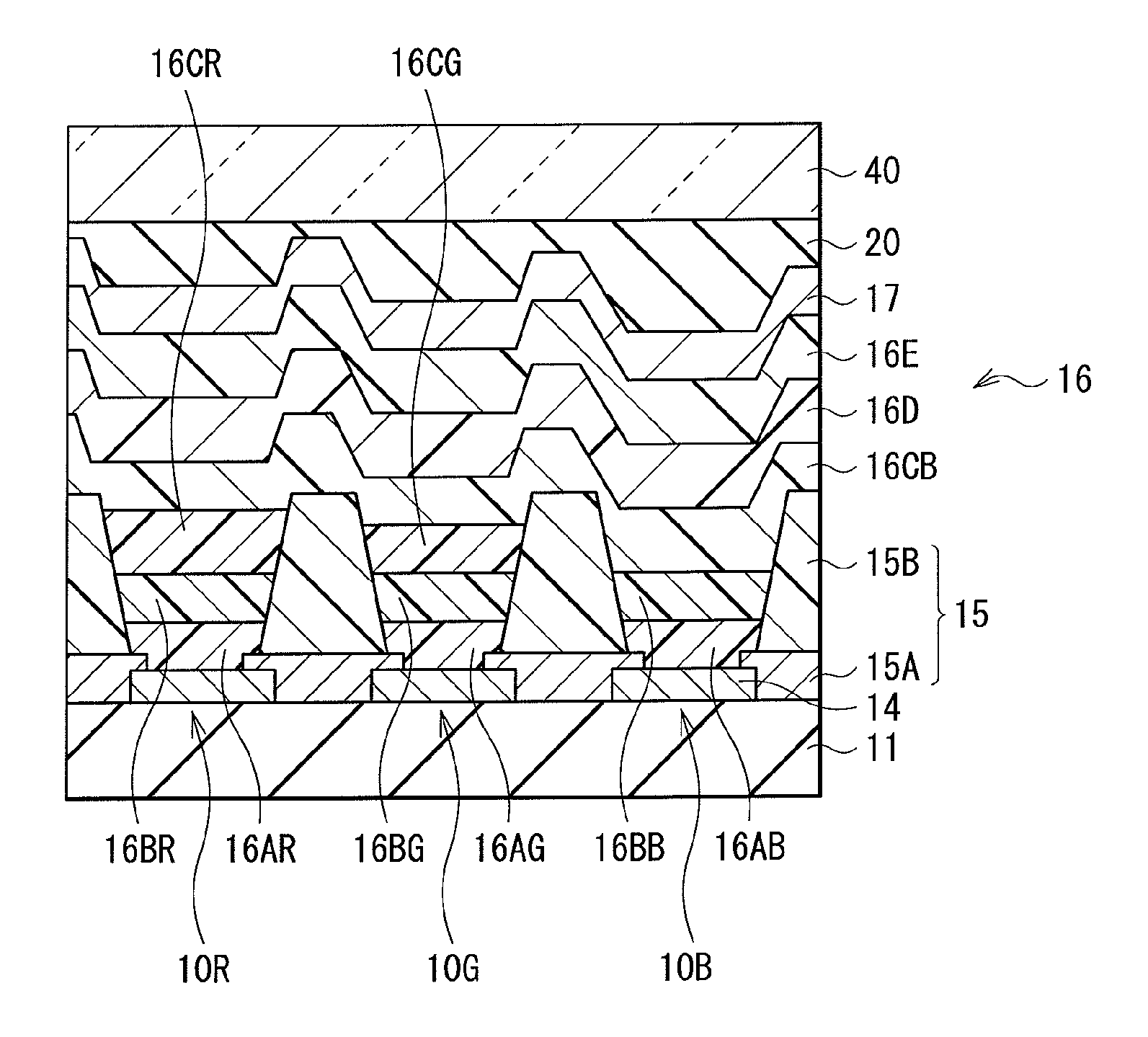
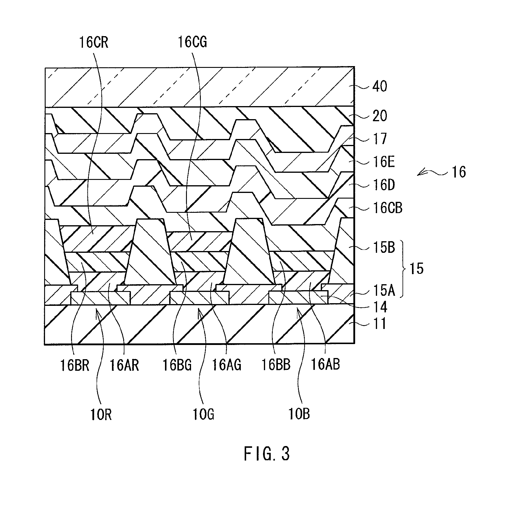
An organic EL display includes: lower electrodes arranged on a substrate so as to correspond to red, green and blue organic EL elements, respectively; hole injection / transport layers arranged on the lower electrodes so as to correspond to the red, green and blue organic EL elements, respectively, the hole injection / transport layers having one or both of hole injection and hole transport properties; red and green organic light-emitting layers arranged on the hole injection / transport layers for the red and green organic EL elements, respectively, and including a low-molecular material; a blue organic light-emitting layer arranged on whole surfaces of the red and green organic light-emitting layers and the hole injection / transport layer for the blue organic EL element; and an electron injection / transport layer and an upper electrode arranged on a whole surface of the blue light-emitting layer, the electron injection / transport layer having one or both of electron injection properties and electron transport properties.

Description

BACKGROUND OF THE INVENTION[0001]1. Field of the Invention[0002]The present invention relates to an organic electroluminescence (EL) display emitting light with use of an organic EL effect, and a method of manufacturing the same.[0003]2. Description of the Related Art[0004]As the development of information and communication industry is accelerated, display elements with higher performance are demanded. An organic EL element attracting attention as a next-generation display element has advantages of not only a wide viewing angle and excellent contract but also fast response time.[0005]Materials of a light-emitting layer and the like forming the organic EL element are broadly divided into low-molecular materials and high molecular materials. It is generally known that the low-molecular materials exhibit high light emission efficiency and a long lifetime, and in particular, performance of low-molecular materials emitting blue light is high.[0006]Moreover, as a method of forming an orga...

Claims


Application Information

Patent Timeline
IPC IPC(8): H01J1/62H01J9/00
CPCH01L27/3211H01L51/0039H01L51/0043H01L51/0058H01L51/5036H01L51/006H01L51/0081H01L51/5004H01L51/0059H10K59/35H10K85/115H10K85/151H10K85/626H10K85/633H10K85/631H10K85/324H10K50/11H10K2101/40H10K50/125
Inventor HIGO, TOMOYUKIYOSHINAGA, TADAHIKO
Owner JOLED INC
Learn More