Organic el display apparatus and method of manufacturing the same

a technology of electroluminescence and display apparatus, which is applied in the manufacture of electrode systems, electric discharge tubes/lamps, and discharge tubes luminescnet screens, etc., can solve the problems of reduced light emission intensity, reduced display performance, and difficulty in patterning formed auxiliary wiring, etc., and achieves a small number of patterning steps. , the effect of high light extraction efficiency

Inactive Publication Date: 2009-01-08
CANON KK
View PDF4 Cites 124 Cited by
  • Summary
  • Abstract
  • Description
  • Claims
  • Application Information

AI Technical Summary

Benefits of technology

[0027]According to the present invention, the auxiliary wiring and the second electrode can be connected with each other without patterning the organic layer for each pixel or without forming the second electrode at the thickness equal to or larger than the required thickness. Further, it is possible to provide an organic EL display apparatus which is produced by a manufacturing process in which the number of patterning steps is small and which has higher light extraction efficiency.

Problems solved by technology

Thus, there is a problem that reduction in display performance due to a voltage gradient, such as reduction in light emission intensity at the central region of the display surface.
Therefore, it is difficult to pattern the formed auxiliary wiring by photolithography, so it is necessary to pattern the auxiliary wiring using a metal mask during the formation thereof.
When a film is to be patterned using a metal mask during the formation thereof by a vacuum vapor deposition method with a low-resistance material such as a metal material, it is difficult to maintain a constant distance between a substrate and the metal mask and to maintain high patterning precision because the metal material has a high evaporation temperature and the metal mask expands by radiation heat.
In particular, in the case of a high-definition display panel, it is further difficult to perform patterning because a pixel interval is small.
When the organic layer is located between the second electrode and the auxiliary wiring provided between pixels, it is difficult to electrically connect the auxiliary wiring with the second electrode.
In addition, there are problems such as reduction in use efficiency of an expensive organic material used for the organic EL device, which is caused by lengthening a tact time required for film formation, and reduction in yield due to patterning deviation in a patterning step.
However, in the case of the organic EL display apparatus using the organic EL device of the top emission type in which light is extracted from the opposite side to the substrate, it is difficult to obtain high light extraction efficiency due to reduction in light transmittance.

Method used


Image

  • Organic el display apparatus and method of manufacturing the same
  • Organic el display apparatus and method of manufacturing the same
  • Organic el display apparatus and method of manufacturing the same

Examples


Embodiment Construction

[0039]Hereinafter, an exemplary embodiment for carrying out the present invention is described with reference to the attached drawings. However, the present invention is not limited to this embodiment.

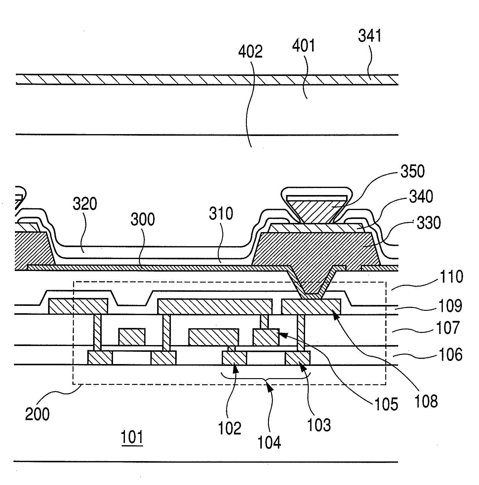
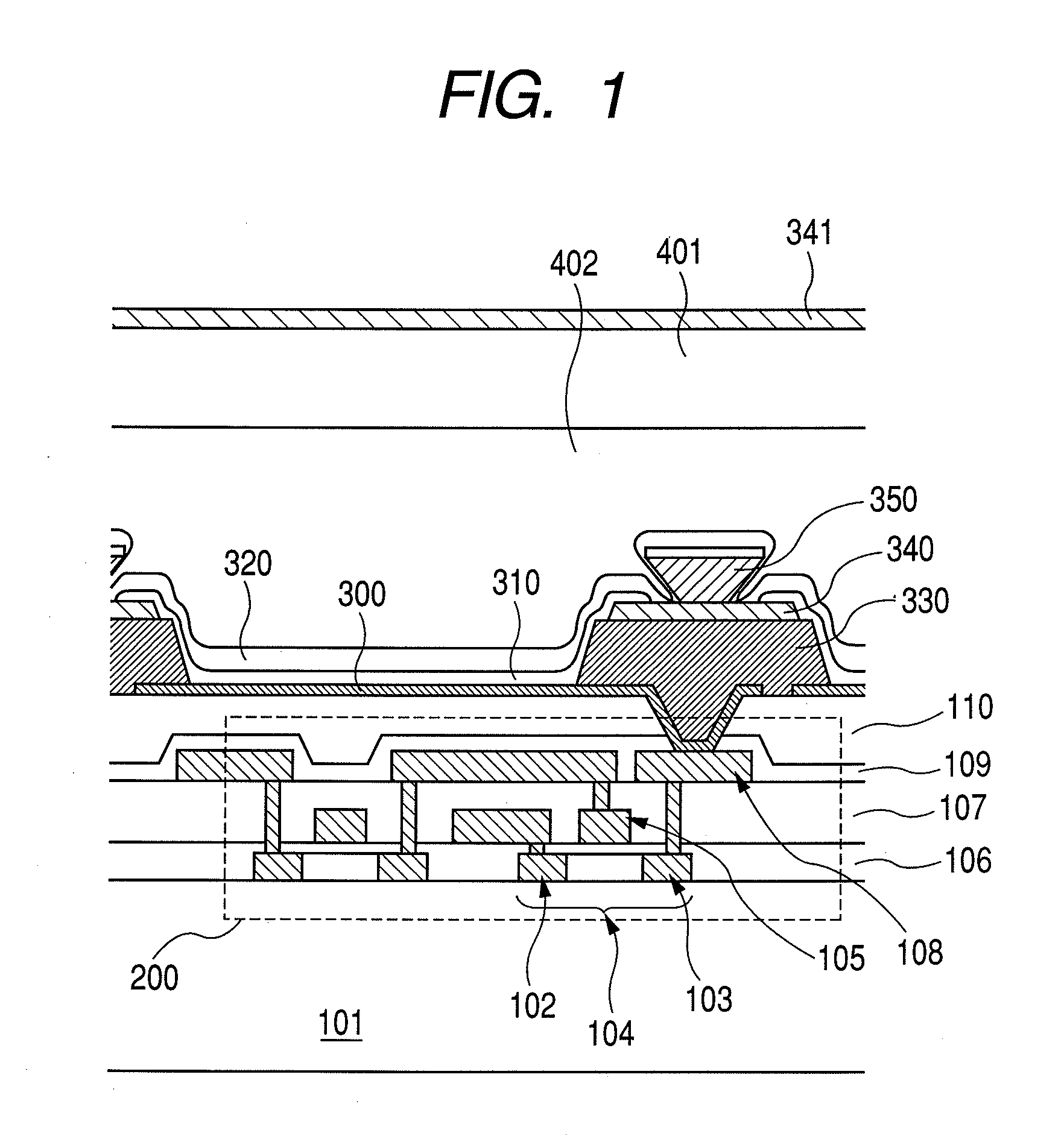
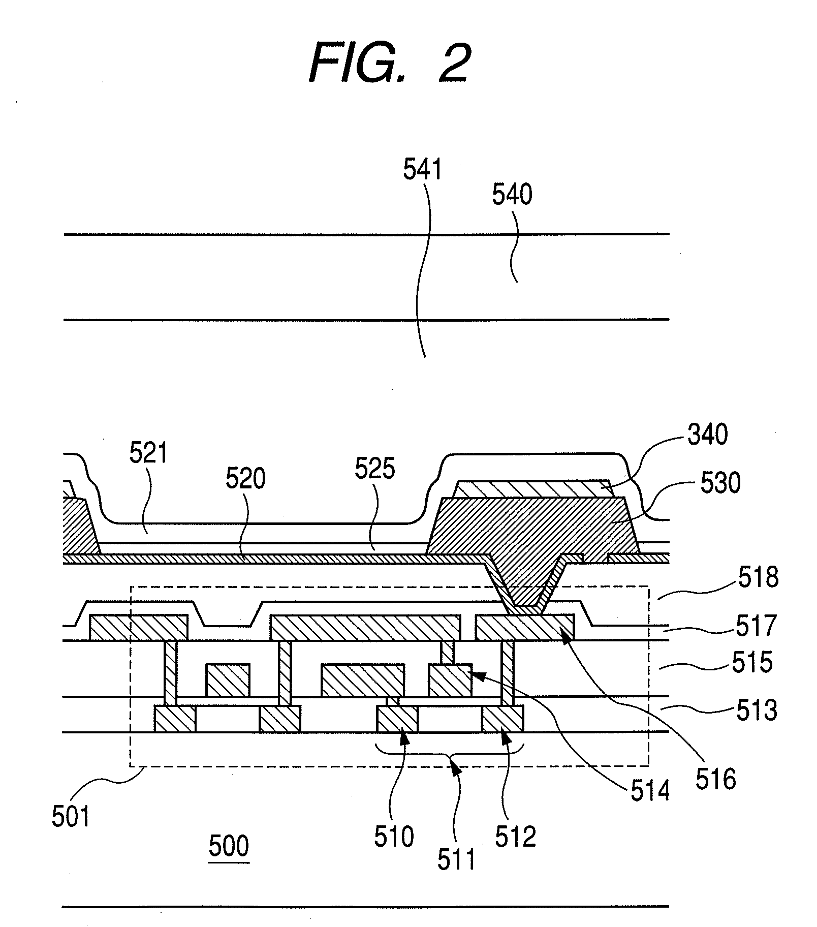
[0040]FIG. 1 is a schematic view illustrating an organic EL display apparatus according to this embodiment. The organic EL display apparatus includes plural organic EL devices each having a first electrode 300, an organic layer 310, and a second electrode 320 which are provided on a substrate 101. The organic layer 310 includes at least a light emitting layer. Organic EL light emitted from the light emitting layer is extracted through the second electrode 320. The organic EL display apparatus further includes: insulating pixel isolation films 330 each of which is provided between the first electrodes located adjacent to each other; and auxiliary wirings 340 which are provided on the pixel isolation films 330 and made of a conductive material.

[0041]The organic EL display apparatus accor...


PUM


Abstract

Provided is an organic EL display apparatus including: a substrate; plural organic EL devices formed over the substrate, each of the organic EL devices including a first electrode, an organic layer, and a second electrode which are provided in order from a side of the substrate, the organic layer including at least a light emitting layer; plural pixel isolation films, each of which is an insulating film and formed between the first electrodes located adjacent to each other; plural auxiliary wirings which are formed on the plural pixel isolation films and include a conductive material; and plural partition walls which are formed on the auxiliary wirings and include one of an insulator and a conductor which is reverse-tapered to have reverse-tapered portions, in which the plural auxiliary wirings and the second electrodes are electrically connected with each other in positions directly under the reverse-tapered portions of the plural partition walls.

Description

BACKGROUND OF THE INVENTION[0001]1. Field of the Invention[0002]The present invention relates to an organic electroluminescence (EL) display apparatus and a method of manufacturing the organic EL display apparatus.[0003]2. Description of the Related Art[0004]In recent years, organic EL display apparatuses using organic EL devices made of light emitting materials are actively developed and studied as display devices having advantages such as a high-speed response and a wide viewing angle.[0005]When an organic EL display apparatus including a large number of organic EL devices is to be driven by an active matrix circuit, it is necessary to connect each of the organic EL devices (pixels) with a set of thin film transistors (TFTs) for controlling a current flowing into each of the pixels.[0006]In the active matrix organic EL display apparatus, minute transistors and capacitors are arranged above a substrate. Therefore, in order to improve an aperture ratio, it is desirable to employ a s...

Claims


Application Information

Patent Timeline
Patent Type & Authority Applications(United States)
IPC IPC(8): H01L51/54H01L51/56
CPCH01L27/3246H01L2251/5315H01L51/5228H10K59/122H10K50/824H10K2102/3026
Inventor TAKATA, KENJI
Owner CANON KK
Why Eureka
Try Eureka