Automatic generating of timing constraints for the validation/signoff of test structures

a technology of automatic generation and validation/signoff, applied in the field of electronic design automation, can solve the problems of unmanageable effort in many designs, inefficient simulation, and inability to verify test structures based on simulation, and achieve the effect of facilitating the debugging of simulation failures

Inactive Publication Date: 2009-02-10
BELL SEMICON LLC
View PDF8 Cites 23 Cited by
  • Summary
  • Abstract
  • Description
  • Claims
  • Application Information

AI Technical Summary

Benefits of technology

[0009]The objects, features and advantages of the present invention include providing a method and / or apparatus for the automatic generation of timing constraints for the validation / signoff of test structures that may (i) facilitate the debugging of simulation failures by keeping timing pictures tightly linked to simulation vectors (e.g., vectors generated by Vecgen®), (ii) assist the user in focusing on real design criticisms, (iii) automatically filter trivial and / or non-real real timing violations, (iv) automate the timing constraint definition to drive physical optimization tools, (v) automate the timing constraint merging process between logic that is shared by the functional design and test structures, (vi) provide an optimal trade-off between timing accuracy and simple constraint description to achieve global optimization in a single-shot run, (vii) increase the design flow robustness by standardizing and automatizing timing setup, (viii) allow a reduction in prototype hold issues, (ix) provide constraint completeness and coverage, (x) provide a detailed description and explanation of the applied constraints, (xi) simplify pattern generation, (xii) simplify simulation runs and / or (xiii) simplify timing results analysis (best vs. worst compare).

Problems solved by technology

With the increasing complexity of designs and multi-million gate technology, verifying test structures based on simulation uses a more significant amount of time.
The effort in many designs is becoming unmanageable.
However, with the increasing complexity of IC designs, performing simulation is not efficient.
Simulation needs long CPU times (matter of days) and the debugging is not easy to perform.
Such long CPU runs are difficult to manage for the typical engineer since the long CPU runs often lead to a significant increase in Turn Around Time.
Such effects are very difficult to be emulated in the simulation environment.
However, STA fails to provide an automatic solution for simplifying (i) timing constraint generation that corresponds to simulation pattern generation, (ii) STA runs and (iii) timing result analysis.
Such redundancy runs the risk of creating errors which can lead to very expensive silicon redesign.
Such a condition will lead to overlapping timing constraints (which produce undesired results) or are completely ignored.
With such conditions, the final result is not what is expected.
Conventional approaches fail to (i) provide a correct timing constraint setup (which is a key point for obtaining a good physical implementation) and (ii) take into account that constraint merging is more complex than file concatenation.

Method used


Image

  • Automatic generating of timing constraints for the validation/signoff of test structures
  • Automatic generating of timing constraints for the validation/signoff of test structures
  • Automatic generating of timing constraints for the validation/signoff of test structures

Examples


Embodiment Construction

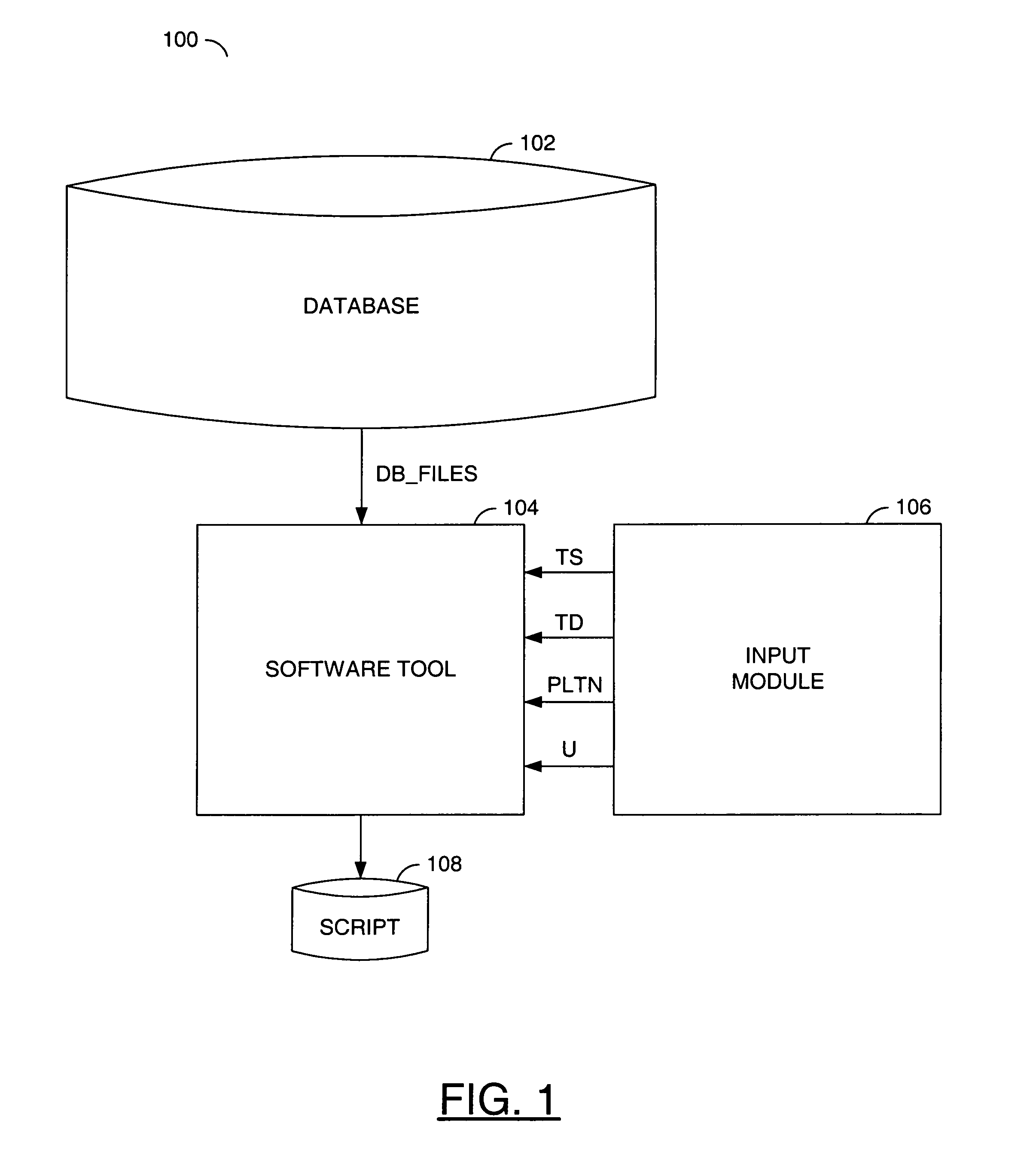
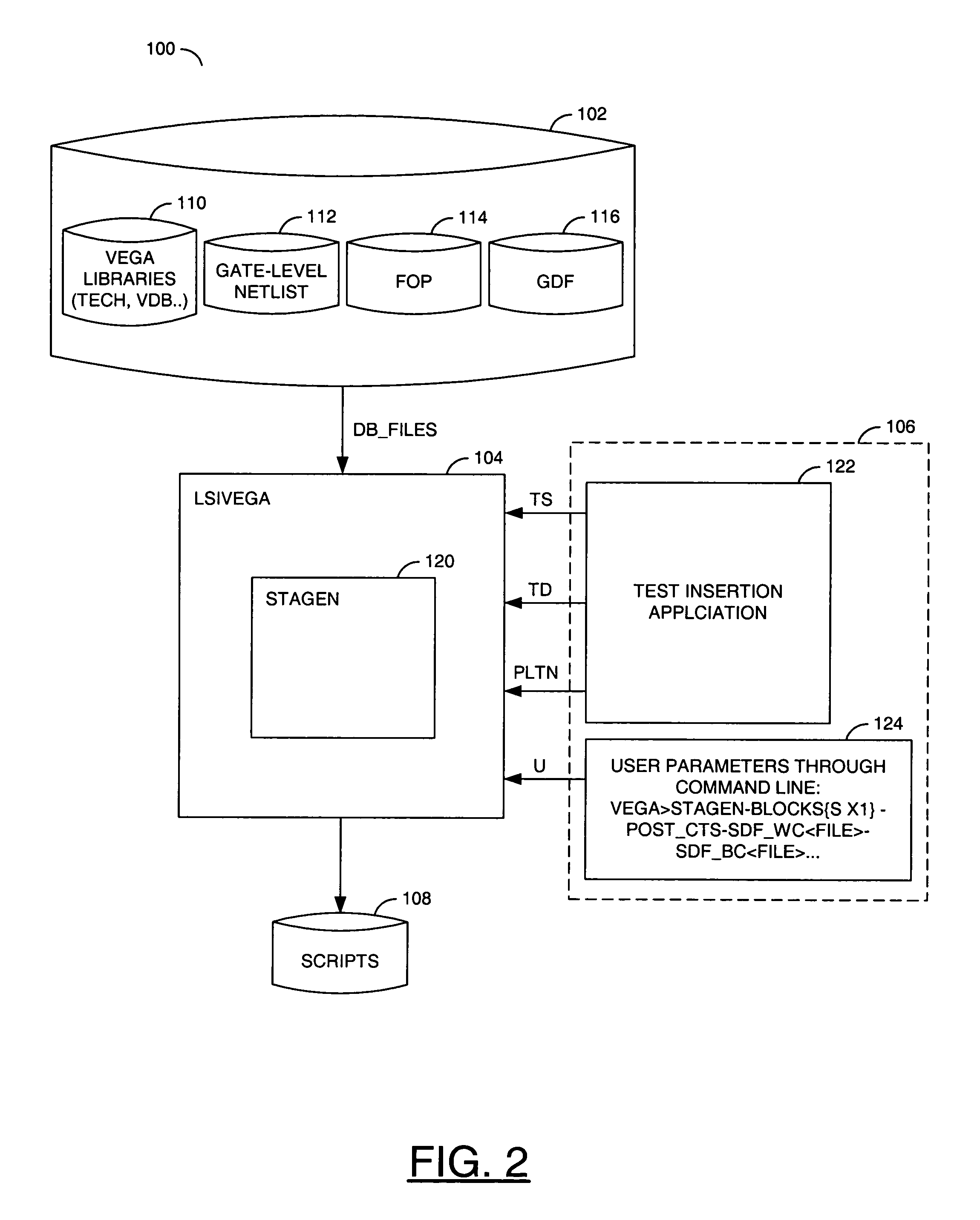
[0017]Referring to FIG. 1, a block diagram of a system 100 is shown in accordance with a preferred embodiment of the present invention. The system 100 generally comprises a database 102, a software tool 104 and an input module 106. The database 102 may present database files (e.g., DB_FILES) to the software tool 104. The input module 106 may present a signal (e.g., TS), a signal (e.g., TD), a signal (e.g., PLTN), and a signal (e.g., U) to the software tool 104. The input module 106 may present information related to test structures over the signal TS. The test structures may be introduced in the design to provide a set of controls for testing predetermined nodes within an ASIC. The test structures may be introduced in the design to guarantee a fault-free IC and to increase the production yield for a customer. Each test structure may include test pins (e.g., both input and output) which may need to be controlled from top level functional pins during manufacturing tests. In general, t...


PUM


Abstract

An apparatus comprising a database, an input module and a software tool. The database may be configured to generate one or more database files representing a design of an integrated circuit (IC). The input module may be configured to generate one or more test structures to test predetermined portions of the design of an IC. The software tool may be configured to automatically generate test scripts to verify timing constraints of the one or more test structures.

Description

FIELD OF THE INVENTION[0001]The present invention relates to electronic design automation (EDA) generally and, more particularly, to a automatic generation of timing constraints for the validation / signoff of test structures.BACKGROUND OF THE INVENTION [0002]With IC designs using conventional technologies, test structures are added into a functional IC design to improve yields. Several test structures, like the scan chain, the memory built-in self test (BIST) / built-in self repair (BISR) and Joint Test Access Group (JTAG) are simultaneously adopted to improve such yields. Such test structures are run at high frequencies in order to (i) minimize test time and (ii) accurately reveal manufacturing defects.[0003]With the increasing complexity of designs and multi-million gate technology, verifying test structures based on simulation uses a more significant amount of time. The effort in many designs is becoming unmanageable. Recent test methodologies have been greatly enriched to provide m...

Claims


Application Information

Patent Timeline
Patent Type & Authority Patents(United States)
IPC IPC(8): G06F9/45G06F17/50
CPCG06F17/5031G06F30/3312
Inventor FOMACIARI, GIUSEPPEMAZZA, FABIOLU, CAM LUONGSHEN, WILLIAM
Owner BELL SEMICON LLC
Why Eureka
Try Eureka