Interposer and test assembly for testing electronic devices

a technology for electronic devices and test assemblies, applied in the direction of individual semiconductor device testing, printed circuit aspects, instruments, etc., can solve the problems of physical limitations, limited probe arrangement, and difficulty in fabricating adequate probe arrays, so as to enhance the art of testing semiconductor chips

Inactive Publication Date: 2009-03-10
TTM TECH NORTH AMERICA LLC
View PDF31 Cites 38 Cited by
  • Summary
  • Abstract
  • Description
  • Claims
  • Application Information

AI Technical Summary

Benefits of technology

[0035]It is, therefore, a primary object of the present invention to enhance the art of testing semiconductor chips.
[0036]It is another object of the invention to provide an improved interposer structure adaptable for use between at least one chip (and possibly a wafer of same) and a printed circuit board.
[0037]It is yet another object of the invention to provide such a structure which is compressible, thereby accommodating for non-planarity of the chip and / or printed circuit board contacts to thus assure that a sound connection is completed to all such contacts.

Problems solved by technology

These probe arrangements, however, have limitations, including, for example, a physical limitation due to the size differential between the relatively less dense pattern of contacts or conductors of the printed circuit board used for electrical testing and the higher dense pattern of contact sites (contacts) on the semiconductor chip.
Thus, with the increasing density of contacts on chips, for example, it becomes more and more difficult to fabricate probe arrays with probe densities adequate to make proper electrical connection to a chip, wafer or substrate.
Another limitation to known probe arrangements resides in the limitations on the clock speed of such connections.
Yet another limitation, related to the first above, is the limited space for each of the test probes to effectively engage the respective contact on the device.
Finally, yet another limitation is the need to be able to effectively orient the interposer on the test PCB with sound contact to the PCB's upper surface conductors.

Method used


Image

  • Interposer and test assembly for testing electronic devices
  • Interposer and test assembly for testing electronic devices
  • Interposer and test assembly for testing electronic devices

Examples


Embodiment Construction

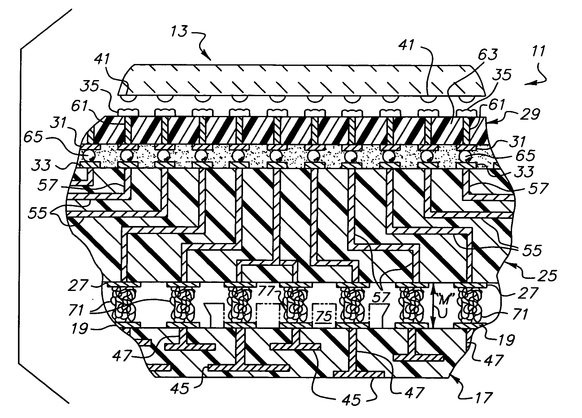
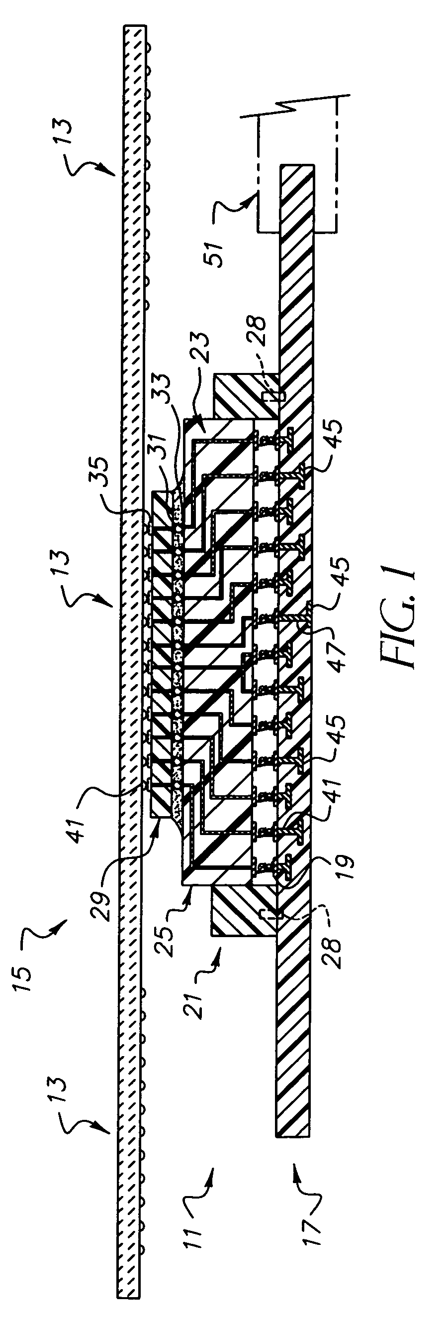
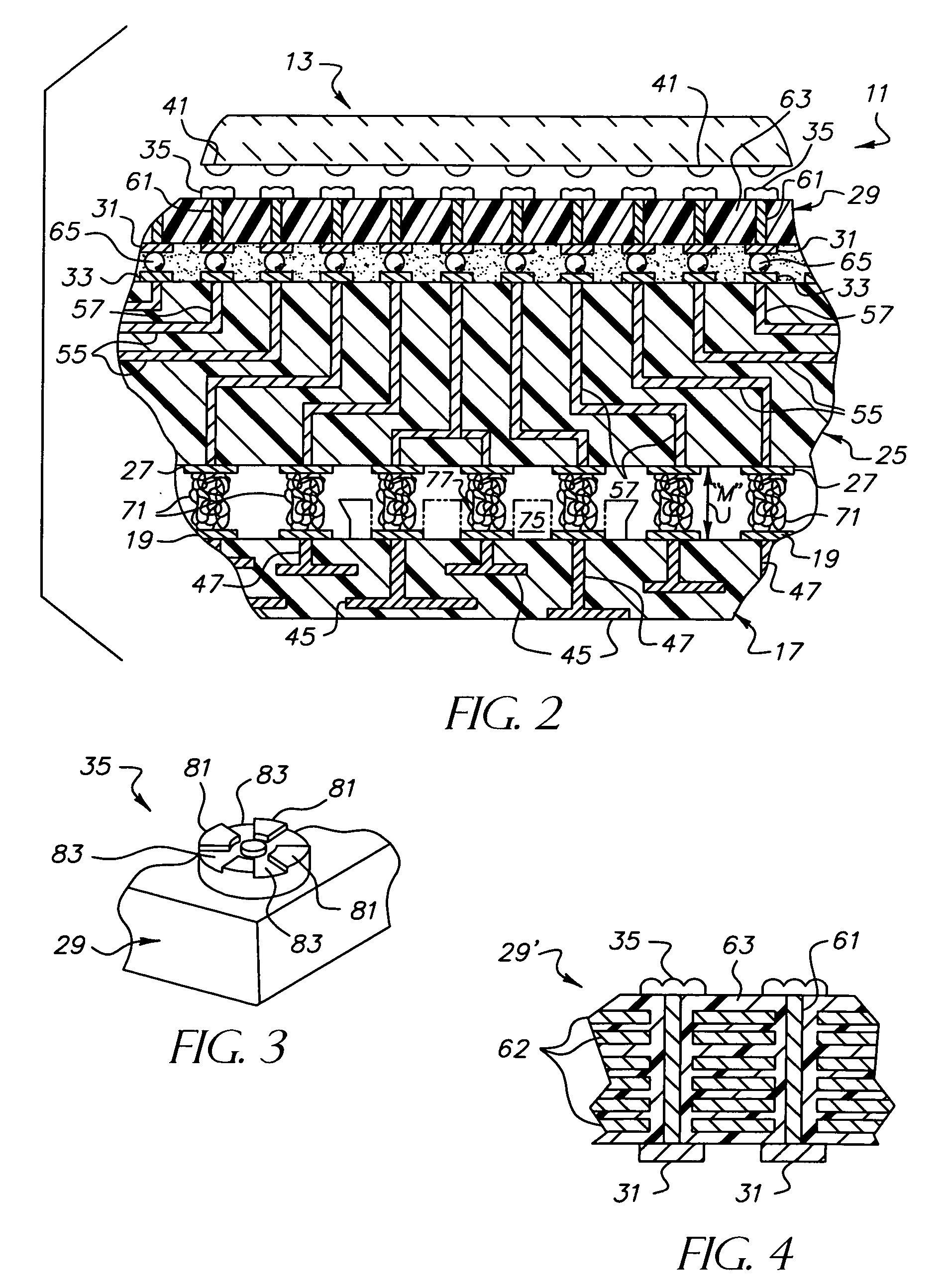
[0045]For a better understanding of the present invention, together with other objects, advantages and capabilities thereof, reference is made to the following disclosure and appended claims in connection with the above-described drawings. It is understood that like numerals will be used to indicate like elements in the FIGS. presented.

[0046]By the term “circuitized substrate” as used herein is meant to include a substrate which includes at least one dielectric layer and a plurality of internal conductive lines which function to interconnect selected ones of a plurality of conductors on one side of the substrate with those on an opposite side. Examples of dielectric materials include such materials as fiberglass-reinforced epoxy resins (some referred to as “FR-4” dielectric materials in the art), polytetrafluoroethylene (PTFE, one example being Teflon, a well known product sold by E.I. duPont deNemours & Company, also the owner of this trademark), polyimides, polyamides, cyanate res...


PUM


Abstract

A test apparatus which uses a pair of substrates and housing to interconnect a host substrate (e.g., PCB) to an electronic device (e.g., semiconductor chip) to accomplish testing of the device. The apparatus includes a housing designed for being positioned on the PCB and have one of the substrates oriented therein during device engagement. The engaging contacts of the upper (second) substrate are sculpted to assure effective chip connection.

Description

CROSS REFERENCE TO CO-PENDING APPLICATION[0001]U.S. Pat. No. 7,292,055 entitled “Interposer For Use With Test Apparatus And Method Of Making Said Interposer” (inventors: F. Egitto et al), an interposer is disclosed comprising at least two dielectric layers bonded to each other, sandwiching a plurality of conductors there-between. The conductors each electrically couple a respective pair of opposed electrical contacts formed within and protruding from openings with the dielectric layers. The interposer is ideally suited for use as part of a test apparatus to interconnect highly dense patterns of solder ball contacts of a semiconductor chip to lesser dense arrays of contacts on the apparatus's printed circuit board. The interposer is also capable of being used for other purposes, including as an interconnecting circuitized substrate between a semiconductor chip and a chip carrier substrate or between a chip carrier and a printed circuit board. Various methods of making such an interpo...

Claims


Application Information

Patent Timeline
Patent Type & Authority Patents(United States)
IPC IPC(8): G01R31/02
CPCG01R1/06711G01R1/0735H05K3/4007H05K1/0393H05K3/365H05K2201/0367H05K2201/0394H05K2201/09627H05K2201/09745H05K2201/10378G01R1/07378
Inventor CHAN, BENSONEGITTO, FRANK D.MARKOVICH, VOYA R.
Owner TTM TECH NORTH AMERICA LLC
Why Eureka
Try Eureka