Light-emitting element and light emitting device using the same

a technology of light-emitting elements and light-emitting devices, which is applied in the field of light-emitting elements, can solve the problems of increasing the driving voltage with the accumulation of light-emission time, and achieve the effects of less increase in resistance value, high reliability, and less increase in driving voltag

Active Publication Date: 2009-07-21
SEMICON ENERGY LAB CO LTD
View PDF23 Cites 47 Cited by
  • Summary
  • Abstract
  • Description
  • Claims
  • Application Information

AI Technical Summary

Benefits of technology

[0005]It is an object of the present invention to provide a light-emitting element having less increase in driving voltage with the accumulation of light-emission time. It is another object of the present invention to provide a light-emitting element having less increase in resistance value with the increase in film thickness.
[0013]According to the present invention, a highly reliable light-emitting element having less increase in driving voltage with the accumulation of light-emission time can be obtained.
[0014]In addition, a light-emitting element having less increase in resistance value depending on the thickness of a layer generating holes, can be obtained according to the present invention. As a result, a light-emitting element in which a distance between electrodes can be changed easily, can be obtained. Also, a short circuit between the electrodes, due to unevenness of the surfaces of the electrodes, can be prevented by increasing the distance between the electrodes. Additionally, by controlling the distance between the electrodes, an optical distance can be easily controlled such that a maximum light-extraction efficiency can be obtained. In addition, by controlling the distance between the electrodes, an optical distance can be controlled easily so that the variation in emission spectrum depending on the angle between the light-extraction surface and the viewer's line of sight is reduced.
[0015]Furthermore, by applying a light-emitting element obtained according to the present invention to a light-emitting device, a highly reliable light-emitting device that can withstand long-time use can be obtained. Moreover, by applying the light-emitting element obtained according to the present invention, to a light-emitting device having a display function, it is possible to obtain a light-emitting device in which light can be emitted to the outside efficiently, and which can display high-definition images with smaller variation in the emission spectrum depending on the angle between the light-extraction surface and the viewer's line of sight.

Problems solved by technology

A large number of these light-emitting elements have a problem in that the driving voltage is increased with the accumulation of light-emission time.

Method used


Image

  • Light-emitting element and light emitting device using the same
  • Light-emitting element and light emitting device using the same
  • Light-emitting element and light emitting device using the same

Examples


embodiment mode 1

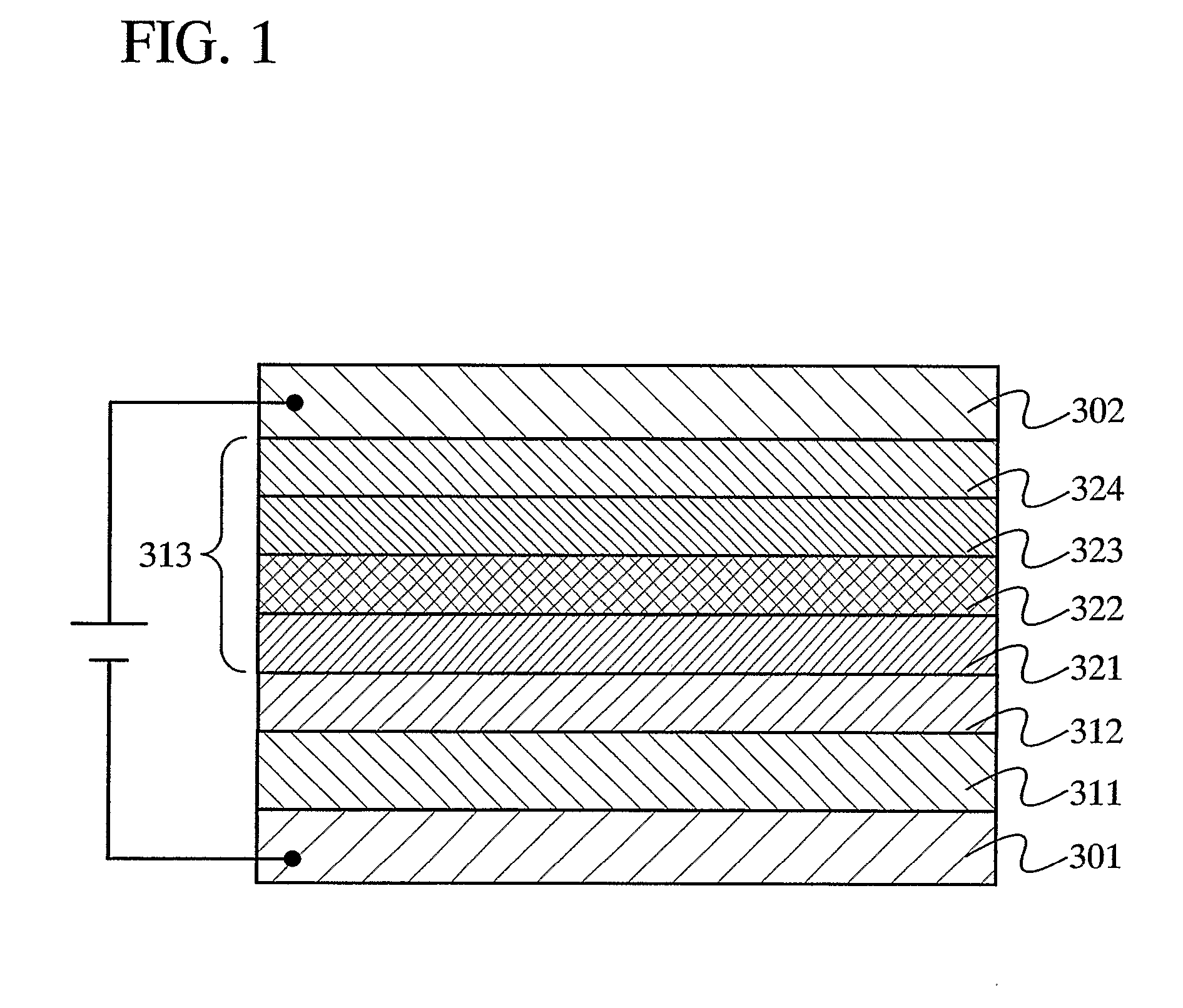
[0048]One mode of the present invention will be described with reference to a cross sectional view of a light-emitting element as shown in FIG. 1.

[0049]The light-emitting element includes a first layer 311, a second layer 312 and a third layer 313 between a first electrode 301 and a second electrode 302. The first layer 311, the second layer 312 and the third layer 313 are stacked sequentially. The first layer 311 is in contact with the first electrode 301 and the third layer 313 is in contact with the second electrode 302.

[0050]The light-emitting element of this embodiment mode is operated as follows. When voltage is applied such that a potential of the second electrode 302 is higher than that of the first electrode 301, holes are injected into the first electrode 301 from the first layer 311 while electrons are injected into the third layer 313 from the second layer 312. Also, holes are injected into the third layer 313 from the second electrode 302. The holes injected from the se...

embodiment mode 2

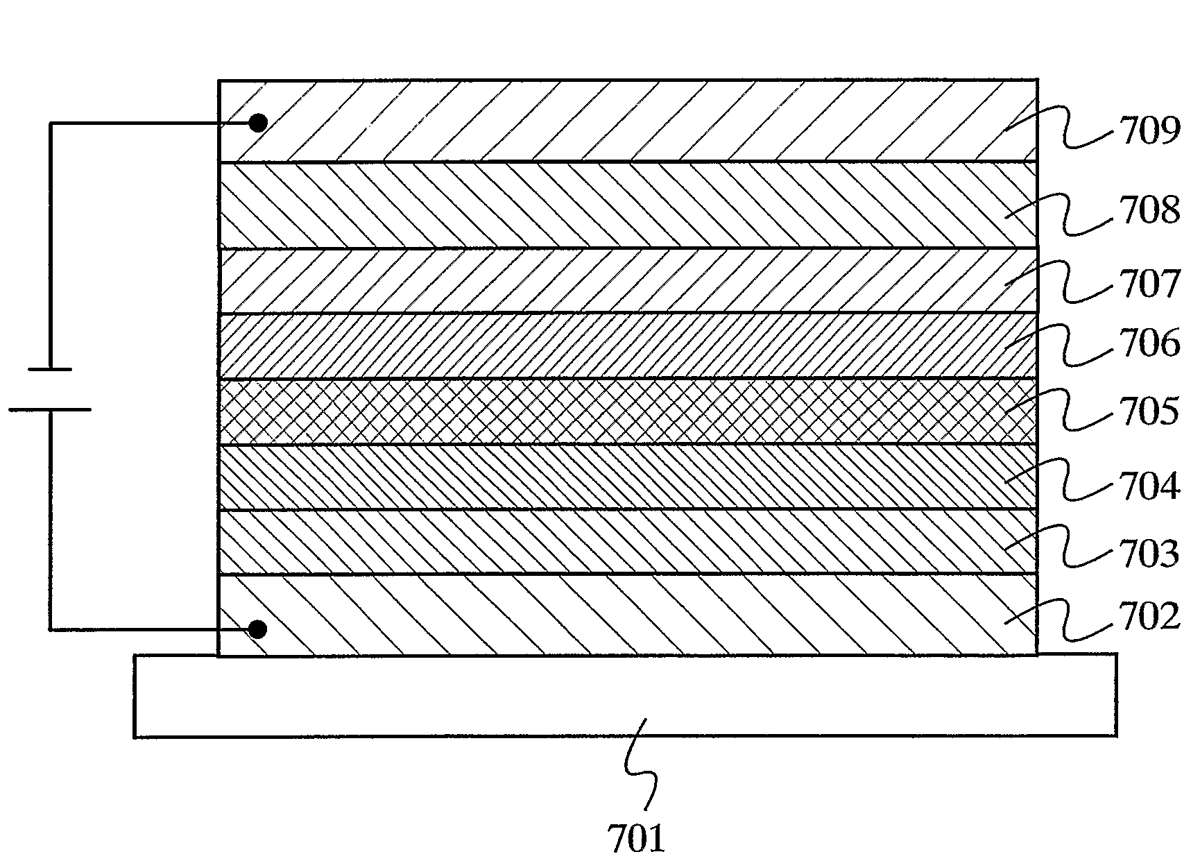
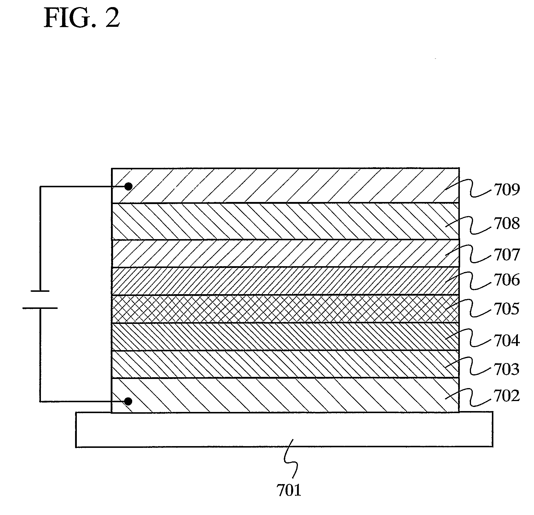
[0071]This embodiment mode will describe a light-emitting element in which, by controlling the thickness of a layer generating holes, a light extraction efficiency is increased and an optical distance between an reflecting surface and a light-extraction surface (or a light-emitting region) is controlled to reduce changes in emission spectrum depending on an angle between the light-extraction surface and the viewer's line of sight, with reference to FIG. 24.

[0072]A light-emitting element shown in FIG. 24 comprises a first layer 211 generating holes, a second layer 212 generating electrons, and a third layer 213 containing a light-emitting substance between a first electrode 201 and a second electrode 202. The first layer 211, the second layer 212 and the third layer 213 are stacked sequentially with the second layer 212 interposed between the first and third layers. The first layer 211 is in contact with the first electrode 201 while the third layer 213 is in contact with the second ...

embodiment mode 3

[0091]The light-emitting element of the present invention is a highly reliable element having less increase in the driving voltage with the accumulation of light-emission time. Thus, by applying a light-emitting element of the present invention to, e.g., a pixel portion, a light-emitting device having lower power consumption can be obtained. Also, the light-emitting element of the present invention can prevent a short circuit between electrodes easily. Therefore, by applying a light-emitting element of the present invention to a pixel portion, a light-emitting device capable of displaying favorable images having less defects due to a short circuit can be obtained. Furthermore, the light-emitting element of the present invention can easily increase extraction efficiency of light. By applying a light-emitting element of the present invention to a pixel portion, a light-emitting device capable of performing display operation at low power consumption can be obtained.

[0092]In this embodi...


PUM


Abstract

The present invention provides a light-emitting element having less increase in driving voltage with the accumulation of light-emission time, and provides a light-emitting element having less increase in resistance value with the increase in film thickness. A light-emitting element includes a first layer, a second layer and a third layer between a first electrode and a second electrode. The first layer is provided to be closer to the first electrode than the second layer, and the third layer is provided to be closer to the second electrode than the second layer. The first layer is a layer including an aromatic amine compound and a substance showing an electron accepting property to the aromatic amine compound. The second layer includes a substance of which an electron transporting property is stronger than a hole transporting property, and a substance showing an electron donating property to the aforementioned substance.

Description

TECHNICAL FIELD[0001]The present invention relates to a light-emitting element comprising a layer including a light-emitting substance between a pair of electrodes, and in particular, relates to a structure of a light-emitting element.BACKGROUND ART[0002]In recent years, a large number of light-emitting elements used for display devices and the like each have a structure in which a layer including a light-emitting substance is sandwiched between a pair of electrodes. Such a light-emitting element emits light when an excited electron, which is formed by a recombination of an electron injected from one electrode and a hole injected from the other electrode, returns to a ground state.[0003]A large number of these light-emitting elements have a problem in that the driving voltage is increased with the accumulation of light-emission time.[0004]In order to solve this problem, for example, the patent document 1 discloses an organic EL element using a compound with a certain structure, wher...

Claims


Application Information

Patent Timeline
Patent Type & Authority Patents(United States)
IPC IPC(8): H01L35/24H01L51/50H05B33/26
CPCH01L51/50H01L51/5088H01L51/5092H01L27/3244H01L27/3281H01L51/0051H01L51/0061H01L51/0071H01L2251/558H01L51/5262H01L51/0077Y10S257/918H10K59/17H10K59/12H10K85/611H10K85/636H10K85/30H10K85/657H10K50/17H10K50/171H10K50/00H10K50/85H10K2102/351
Inventor KUMAKI, DAISUKESEO, SATOSHI
Owner SEMICON ENERGY LAB CO LTD
Why Eureka
Try Eureka