Method of driving plasma display panel
a technology of plasma display panel and display panel, which is applied in the direction of color television details, television systems, instruments, etc., can solve the problems of deteriorating image display quality and reducing contras
- Summary
- Abstract
- Description
- Claims
- Application Information
AI Technical Summary
Benefits of technology
Problems solved by technology
Method used
Image

Examples
first exemplary embodiment
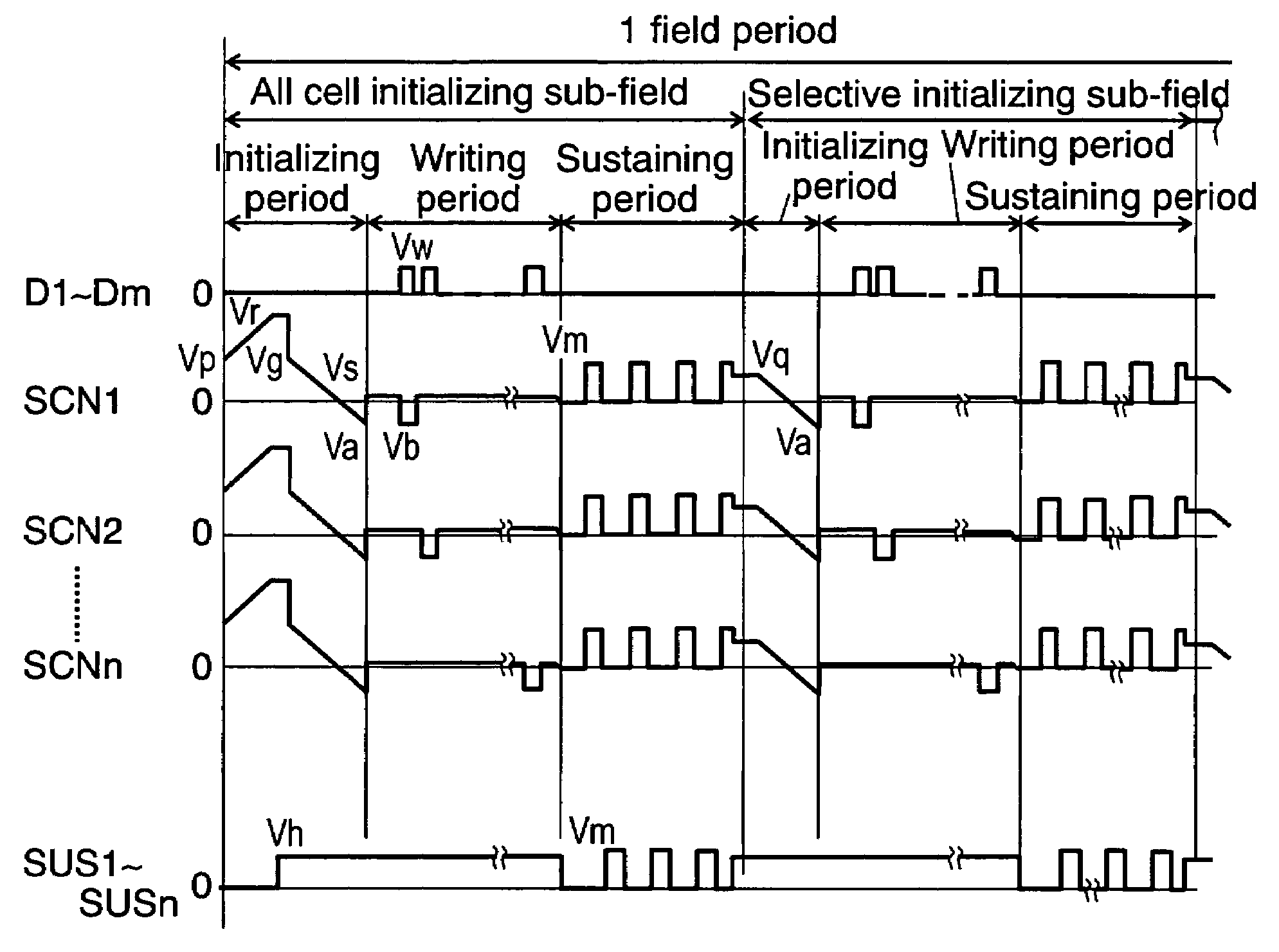
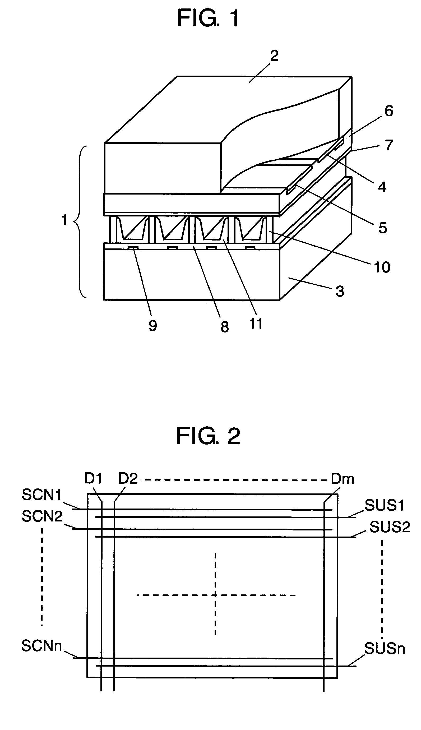
[0023]FIG. 1 is a perspective view illustrating an essential part of a panel for use in the first exemplary embodiment of the present invention. Panel 1 is composed of front substrate 2 and rear substrate 3 that are made of glass and faced with each other so as to form a discharge space therebetween. On front substrate 2, a plurality of display electrodes, each formed of a pair of scan electrode 4 and sustain electrode 5, is formed in parallel with each other. Dielectric layer 6 is formed to cover scan electrodes 4 and sustain electrodes 5. On dielectric layer 6, protective layer 7 is formed. On the other hand, on rear substrate 3, a plurality of data electrodes 9 covered with insulating layer 8 is provided. Barrier ribs 10 are provided on insulating layer 8 between data electrodes 9 in parallel therewith. Also, phosphor layers 11 are provided on the surface of insulating layer 8 and the side faces of barrier ribs 10. Front substrate 2 and rear substrate 3 are faced with each other ...
second exemplary embodiment
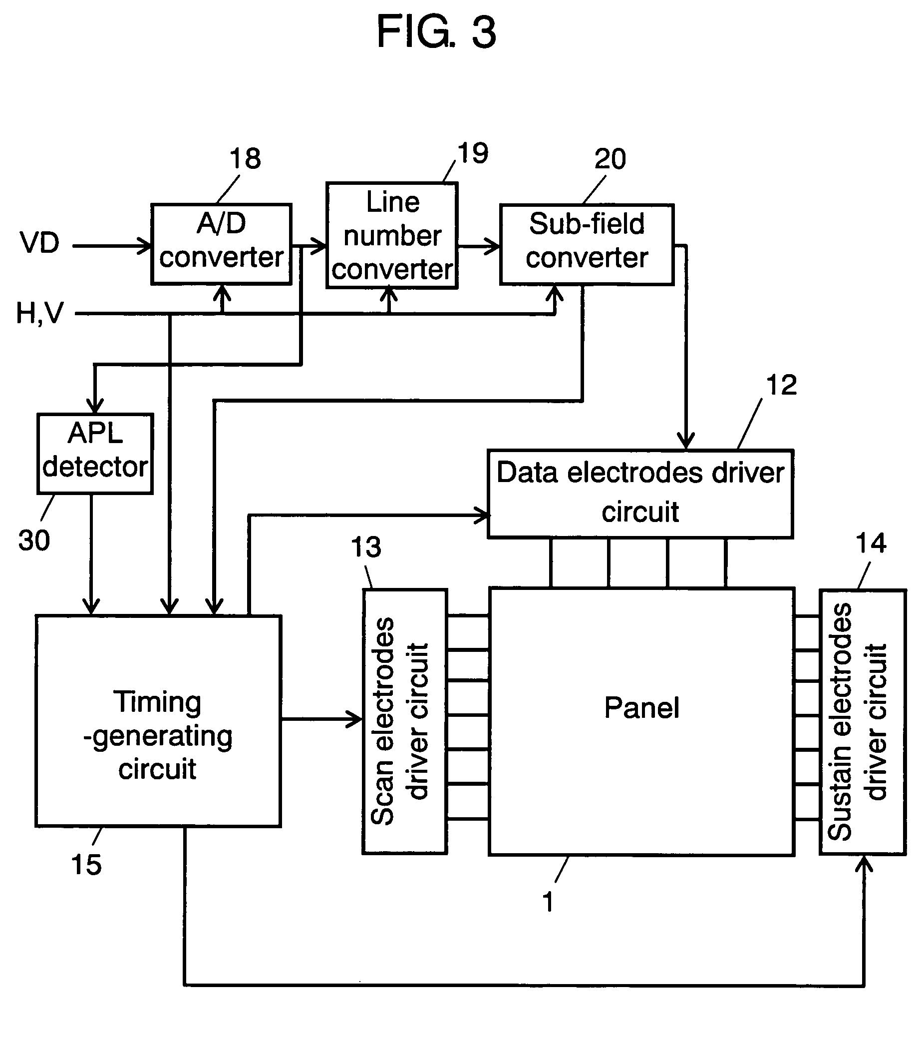
[0047]The essential part of a panel and the array of electrodes for use in the second exemplary embodiment are similar to those of the first exemplary embodiment. Thus, the description thereof is omitted. FIG. 6 is a circuit block diagram of a plasma display device for use in a method of driving a panel in accordance with the second exemplary embodiment. The same elements used in the first exemplary embodiment are denoted with the same reference marks and the description thereof is omitted.
[0048]Sub-field converter 20 divides image data of each pixel into a plurality of bits corresponding to a plurality of sub-fields (SFs), and supplies the image data per SF to data electrodes driving circuit 12 and light-emitting rate detector 31. Light-emitting rate detector 31 detects a light-emitting rate of a predetermined SF, i.e. the light-emitting rate of the 10th SF in this secondary exemplary embodiment.
[0049]Timing-generating circuit 15 generates timing signals based on horizontal synchro...
PUM
 Abstract
Description
Claims
Application Information
 - R&D
- Intellectual Property
- Life Sciences
- Materials
- Tech Scout
- Unparalleled Data Quality
- Higher Quality Content
- 60% Fewer Hallucinations
Browse by: Latest US Patents, China's latest patents, Technical Efficacy Thesaurus, Application Domain, Technology Topic, Popular Technical Reports.
© 2025 PatSnap. All rights reserved.Legal|Privacy policy|Modern Slavery Act Transparency Statement|Sitemap|About US| Contact US: help@patsnap.com