Method for controlling access to a multibank memory

a multi-bank memory and access control technology, applied in the direction of memory adressing/allocation/relocation, digital storage, instruments, etc., can solve the problem that all of the above solutions have in common that they are very costly

Inactive Publication Date: 2009-11-03
THOMSON LICENSING SA
View PDF10 Cites 3 Cited by
  • Summary
  • Abstract
  • Description
  • Claims
  • Application Information

AI Technical Summary

Benefits of technology

[0014]This method provides a cheap and less complex solution for memory scheduling and controlling. The data buffer is spread over at least two banks, which are linearly accessed. The first bank is filled with the input stream until a read command for this bank is received from a buffer control. In this case the input stream switches to the second bank. If the output stream needs to access the second bank the input stream returns to the first bank. The input stream does not leave its bank until the output stream wants to read the same bank.
[0024]To reliably switch each bank between input and output functionality a complex pointer control is required. By marking the last position of the input stream in the first or the second bank, respectively, the control of the switching process for the output stream is noticeably simplified.
[0030]Advantageously, the method further comprises the step of holding an activated row of a bank open until a refresh cycle is issued or until the end of the row is reached by a burst. This allows to save approximately ten cycles latency for each single access.
[0031]Favorably, the banks are single-port static random access memory modules. In this case input data are written into the first module until a read request is received for this module. The input data are then written into the second module whilst data are read from the first module. Reading and writing is, therefore, performed simultaneously. A further advantage is that instead of a more expensive and complicated dual-port SRAM module of a specific size two single-port SRAM modules with half the size each can be used, e.g. two single-port SRAM modules with 512 bytes each instead of a dual-port SRAM module with 1024 bytes.

Problems solved by technology

All of the above solutions have in common that they are very costly.

Method used


Image

  • Method for controlling access to a multibank memory
  • Method for controlling access to a multibank memory
  • Method for controlling access to a multibank memory

Examples


Embodiment Construction

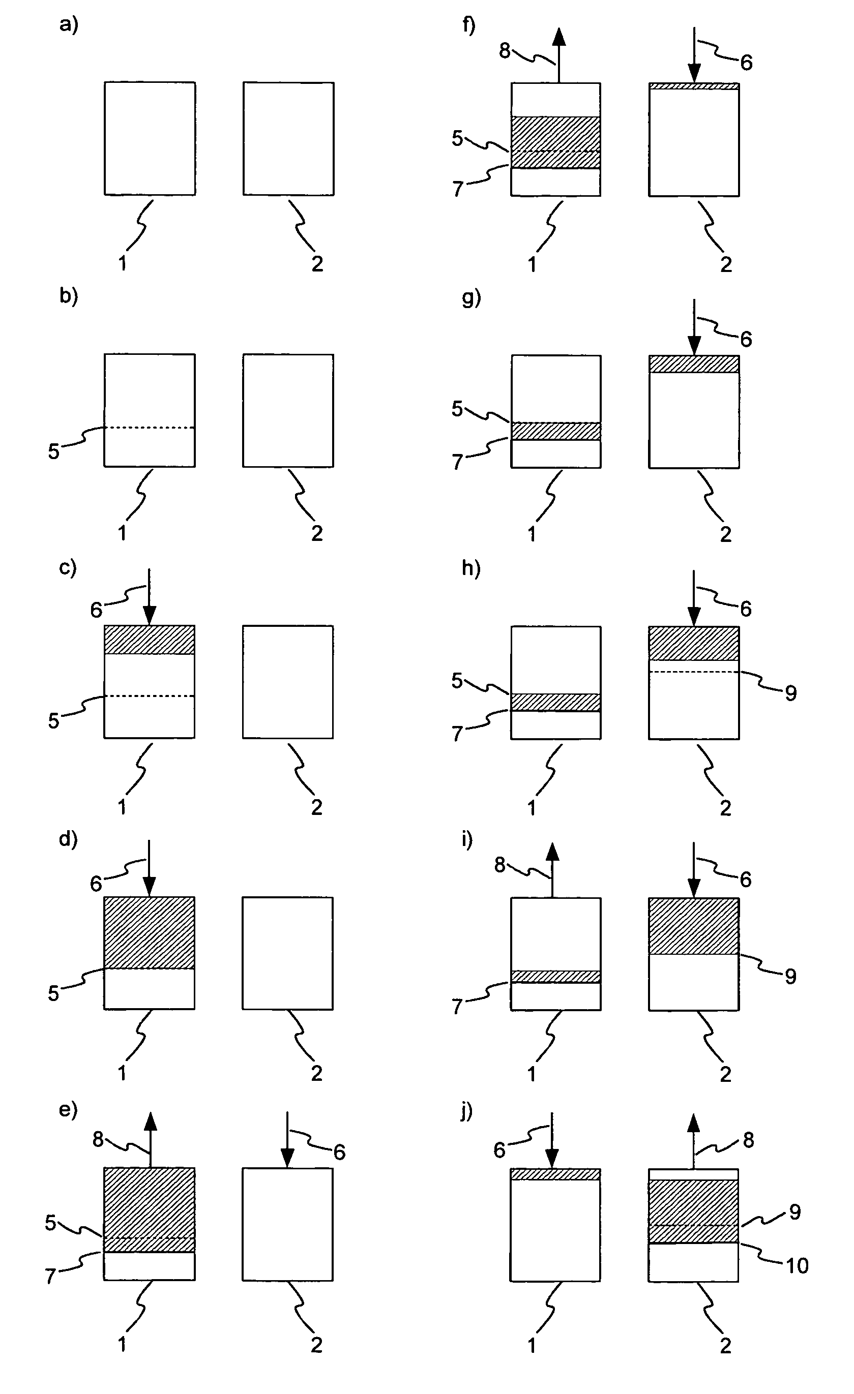
[0043]In FIG. 1 access to two banks 1,2 of an SDRAM using a method according to the invention is shown. For simplicity the access is divided into a sequence of states of the banks, which are depicted in parts a) to j) of FIG. 1. For better clarity in the figure only a single complete output block is written into one bank 1,2. Of course a plurality of output blocks can subsequently be written into the banks. When the access is initiated both banks 1,2 are empty, which corresponds to FIG. 1a). As shown in part b), in the left bank 1 a pointer 5 is set to mark the size of an output block. The input stream 6 coming from the drive are now stored in the left bank 1, which is depicted in part c). As soon as the pointer 5 is reached, the buffer can be read. Until a read access occurs, the writing to the left bank 1 continues. This is shown in part d). In this way the first bank 1 is filled with a plurality of output blocks. After the first read access to the left bank 1 the input stream 6 i...


PUM


Abstract

The present invention relates to a method for scheduling and controlling access to a multibank memory having at least two banks, and to an apparatus for reading from and / or writing to recording media using such method. According to the invention, the method comprises the steps of: writing an input stream to the first bank; switching the writing of the input stream to the second bank when a read command for the first bank is received; and switching the writing of the input stream back to the first bank when a read command for the second bank is received.

Description

[0001]This application claims the benefit, under 35 U.S.C. § 119 of European Patent Application 03019948.3, filed Sep. 2, 2003.FIELD OF THE INVENTION[0002]The present invention relates to a method for scheduling and controlling access to a multibank memory, and to an apparatus for reading from and / or writing to recording media using such method.BACKGROUND OF THE INVENTION[0003]In the following the invention is explained with reference to synchronous dynamical random access memory (SDRAM). However, the invention is applicable to any kind of dynamical random access memory, e.g. double data rate RAM (DDR-RAM), enhanced synchronous DRAM (ESDRAM), synchronous link DRAM (SLDRAM), Rambus DRAM (RDRAM), etc. Furthermore, the invention is also applicable to single-port static random access memory (single-port SRAM).[0004]Typical SDRAM modules comprise four independent banks. Each bank consists of rows, which consist of columns. To access a datum the corresponding row on the corresponding bank...

Claims


Application Information

Patent Timeline
Patent Type & Authority Patents(United States)
IPC IPC(8): G06F12/00G06F12/06G06F12/02G11C7/10G11C11/407
CPCG11C7/1042G06F12/02G06F12/06
Inventor NIGGEMEIER, TIMBRUNE, THOMAS
Owner THOMSON LICENSING SA
Why Eureka
Try Eureka