Semiconductor device having firmly secured heat spreader

a heat spreader and semiconductor technology, applied in the direction of semiconductor devices, semiconductor/solid-state device details, electrical apparatus, etc., can solve the problems of increasing effort, less effective exposed leadframes, and higher energy density, and achieve no investment

Active Publication Date: 2009-12-22
TEXAS INSTR INC
View PDF17 Cites 12 Cited by
  • Summary
  • Abstract
  • Description
  • Claims
  • Application Information

AI Technical Summary

Benefits of technology

[0012]It is a technical advantage of the invention that it offers low-cost design and fabrication options for the leadframe members. The members have shapes resembling elongated protrusions, dimples, or thorns, and project from the planar leadframe at an angle, which is selected between and acute and a right angle. The members are preferably stamped from the planar leadframe sheet.
[0013]It is another technical advantage that the innovation of the invention is accomplished using the installed equipment base for leadframe manufacture so that no investment in new manufacturing machines is needed.

Problems solved by technology

This effort becomes increasingly harder, the higher the energy density becomes.
In application where there is no outside heat sink available, the exposed leadframe becomes less effective when the leadframe metal thickness has to be reduced driven by the trend towards thinner packages.
The approach to add (“drop in”) a heat spreader to the assembled device is generally plagued by the need to stabilize the spreader for the molding process; otherwise, rotational and / or lateral movements may occur during the molding step.

Method used


Image

  • Semiconductor device having firmly secured heat spreader
  • Semiconductor device having firmly secured heat spreader
  • Semiconductor device having firmly secured heat spreader

Examples


Embodiment Construction

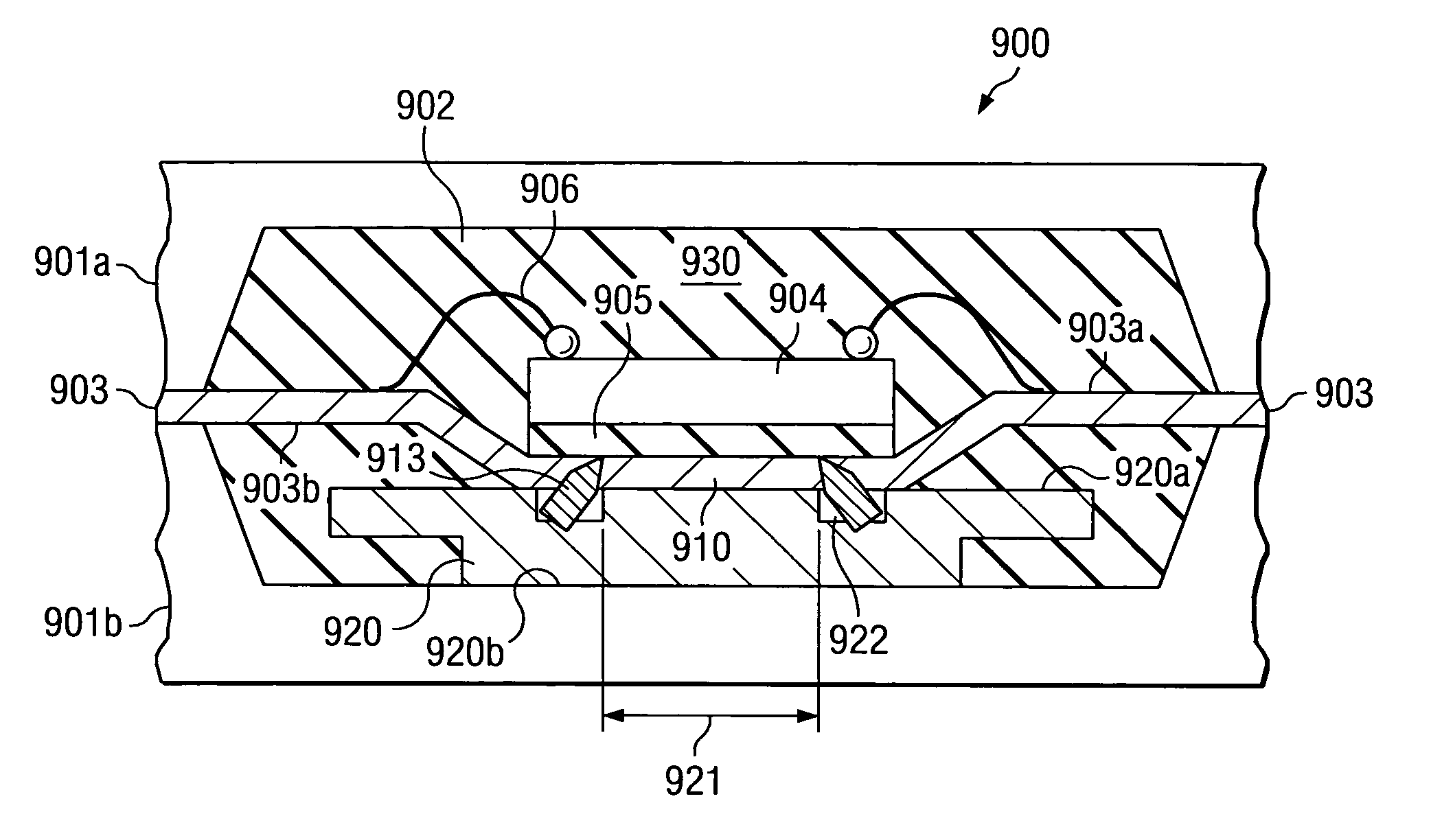
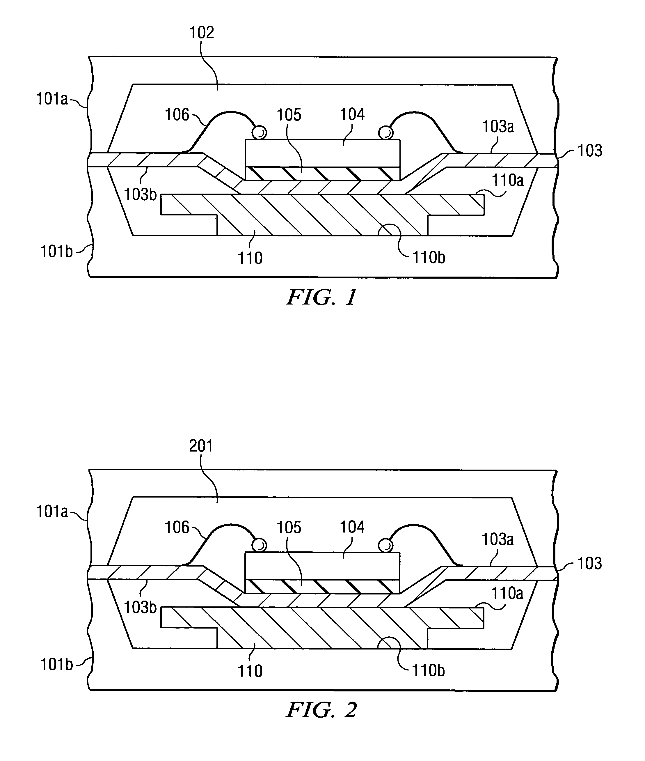
[0036]The schematic cross section of FIG. 1 depicts a stainless steel mold with upper mold half 101a and lower half 101b as commonly used in the transfer molding process of semiconductor device packaging. When placed on top of each other as shown in FIG. 1, the mold halves define the mold cavity 102, which is to be filled with molding compound. A leadframe 103, frequently made of copper, has been loaded in the mold cavity; it is held in place by pressing the mold halves together. On the first surface 103a of leadframe 103 is a semiconductor chip 104 mounted. The mounting step includes the attachment of chip 104 to first leadframe surface 103a using the adhesive 105 (often an epoxy), and the electrical connection of chip bond pads to leadframe segments (only schematically shown in FIG. 1) using connecting wires 106.

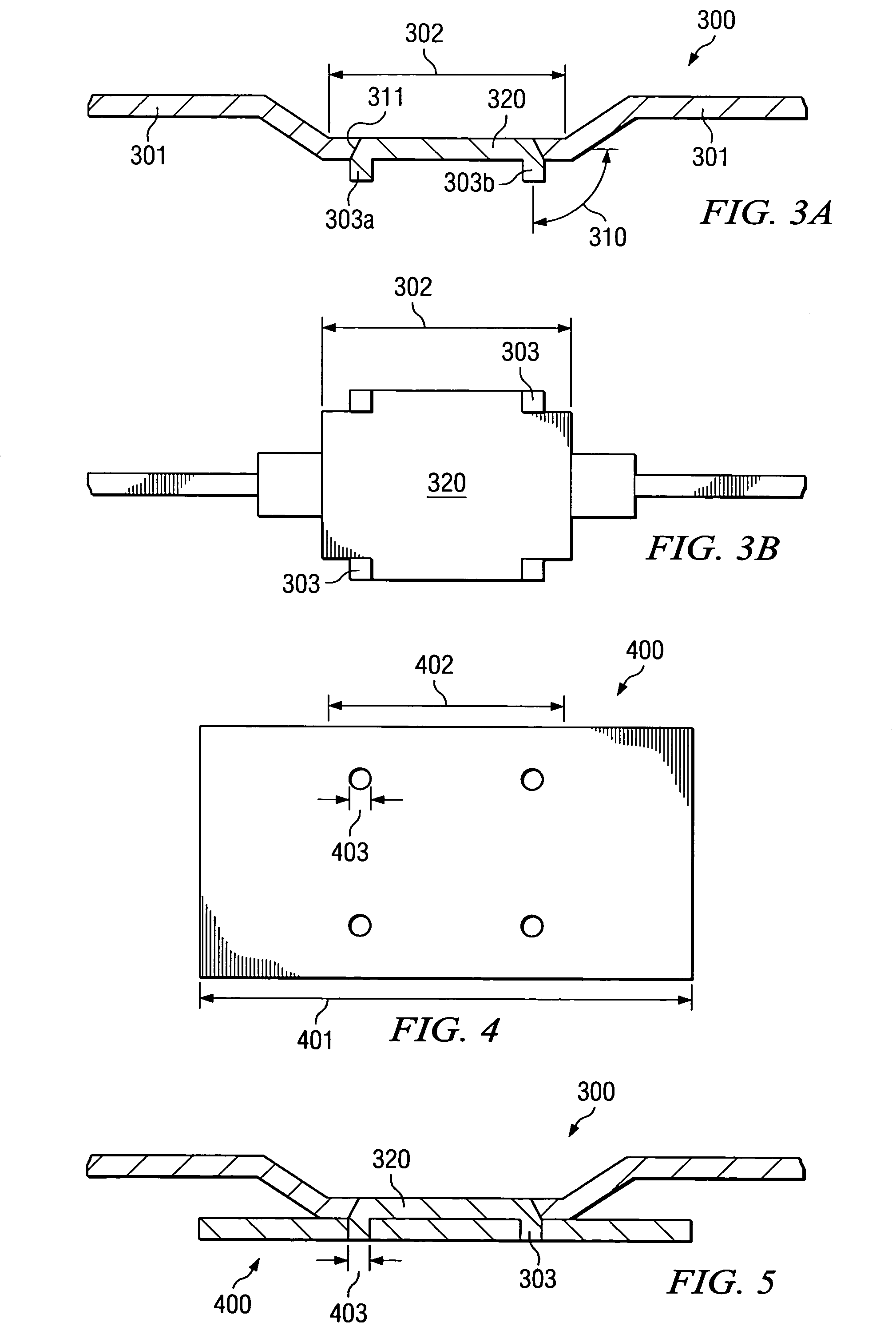
[0037]Heat spreader 110, preferably made of copper, is “dropped in” cavity 102. The first surface 110a of spreader 110 faces second surface 103b of leadframe 103, and the ...


PUM


Abstract

A semiconductor device comprising a leadframe (903), which has first (903a) and second (903b) surfaces, a planar pad (910) of a certain size, and a plurality of non-coplanar members (913) adjoining the pad. The device further has a heat spreader (920) with first (920a) and second (920b) surfaces, a planar pad of a size matching the leadframe pad size, and contours (922), into which the leadframe members are inserted so that the first spreader pad surface touches the second leadframe pad surface across the pad size. A semiconductor chip (904) is mounted on the first leadframe pad surface. Encapsulation material (930), preferably molding compound, covers the chip, but leaves the second spreader surface uncovered.

Description

FIELD OF THE INVENTION[0001]The present invention is related in general to the field of electrical systems and semiconductor devices and more specifically to thermally enhanced semiconductor devices having metallic heat spreaders secured for reliable processing.DESCRIPTION OF THE RELATED ART[0002]Removing the thermal heat generated by active components belongs to the most fundamental challenges in integrated circuit technology. Coupled with the ever shrinking component feature sizes and increasing density of device integration is an ever increasing density of power and thermal energy generation. However, in order to keep the active components at their low operating temperatures and high speed, this heat must continuously be dissipated and removed to outside heat sinks. This effort becomes increasingly harder, the higher the energy density becomes.[0003]In known technology, one approach to heat removal, specifically for devices with metallic leads, focuses on thermal transport throug...

Claims


Application Information

Patent Timeline
Patent Type & Authority Patents(United States)
IPC IPC(8): H01L23/495
CPCH01L21/565H01L23/4334H01L2224/48247H01L2224/48465H01L2224/32245H01L2924/01029H01L2924/01078H01L24/48H01L2224/73265H01L2924/01013H01L2924/00H01L2924/181H01L2924/14H01L2924/00014H01L2924/00012H01L2224/45099H01L2224/45015H01L2924/207H01L23/495H01L23/36
Inventor LANGE, BERNHARD P.KUMMERL, STEVEN A.
Owner TEXAS INSTR INC
Why Eureka
Try Eureka