

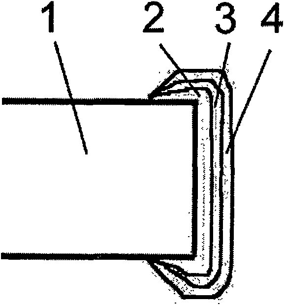
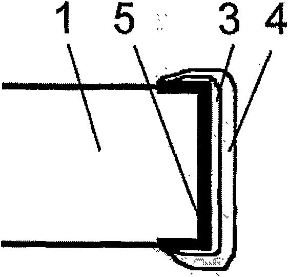
Sheet type ferrite inductor terminal electrode and its preparation method
An inductor and ferrite technology, applied in the field of chip ceramic electronic components, can solve the problems of complex process and cumbersome process, and achieve the effect of simplifying the production process, reducing the production cost and saving precious metal resources.
- Summary
- Abstract
- Description
- Claims
- Application Information
AI Technical Summary
Problems solved by technology
Method used
Image

Examples
Embodiment 1
[0012] Select 100 pieces of sintered nickel-copper-zinc ferrite chip multilayer inductor (MLCI) blanks, the size is 0402 (0.04 inches × 0.02 inches), and the ferrite composition is Ni 0.3 Zn 0.5 Cu 0.2 Fe 2 o 4 , the molar percentage of iron element is 28.6%. Put the chip inductor and the steel ball with a diameter of 0.5mm in the hanging basket, immerse the hanging basket in the sodium sulfate aqueous solution, use the titanium basket as the anode, electrolyze the aqueous solution under vibration conditions, and perform electrochemical atomic hydrogen on the chip inductor. Conductivity modification treatment to prepare the self-body electrode of the chip inductor. The process parameters are as follows:
[0013] Sodium Sulfate (Na 2 SO 4 ) aqueous solution 50 g / L
[0014] Cathode current density 2 amps / square decimeter
[0015] temperature room temperature
[0016] After 0.5 hours, take out the hanging basket, clean the hanging basket, chip inductors and steel balls ...
Embodiment 2
[0033] Select 100 sintered planar hexagonal Co2Z ferrite chip inductor blanks, the size is 0603 (0.06 inches × 0.03 inches), and the ferrite composition is Ba 3 co 2 Fe 24 o 41 , the molar percentage of iron element is 34.3%. Put the chip inductor and the steel ball with a diameter of 1mm in the hanging basket, immerse the hanging basket in the sodium sulfate aqueous solution, use the titanium basket as the anode, electrolyze the aqueous solution under vibration conditions, and perform electrochemical atomic hydrogen conductance on the chip inductor. Modification treatment to prepare the self-body electrode of the chip inductor. The process parameters are as follows:
[0034] Sodium Sulfate (Na 2 SO 4 ) aqueous solution 200 g / l
[0035] Cathode current density 0.5 ampere / square decimeter
[0036] Temperature 50°C
[0037] After 0.5 hours, take out the hanging basket, clean the hanging basket, chip inductors and steel balls with deionized water, then place the hanging ...
PUM
| Property | Measurement | Unit |
|---|---|---|
| electrical resistivity | aaaaa | aaaaa |
| thickness | aaaaa | aaaaa |
Abstract
Description
Claims
Application Information